Datasheet Details
| Part number | ICS8312I |
|---|---|
| Manufacturer | Integrated Circuit Systems |
| File Size | 280.89 KB |
| Description | 1-TO-12 LVCMOS / LVTTL FANOUT BUFFER |
| Datasheet |
 ICS8312I Datasheet ICS8312I Datasheet
|
|
|
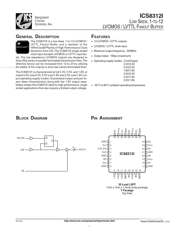
The ICS8312I is a low skew, 1-to-12 LVCMOS / LVTTL Fanout Buffer and a member of the HiPerClockS™ HiPerClockS™family of High Performance Clock Solutions from ICS.
The ICS8312I single ended clock input accepts LVCMOS or LVTTL input levels.
| Part number | ICS8312I |
|---|---|
| Manufacturer | Integrated Circuit Systems |
| File Size | 280.89 KB |
| Description | 1-TO-12 LVCMOS / LVTTL FANOUT BUFFER |
| Datasheet |
ICS8312I Datasheet
|
|
|
|