Description
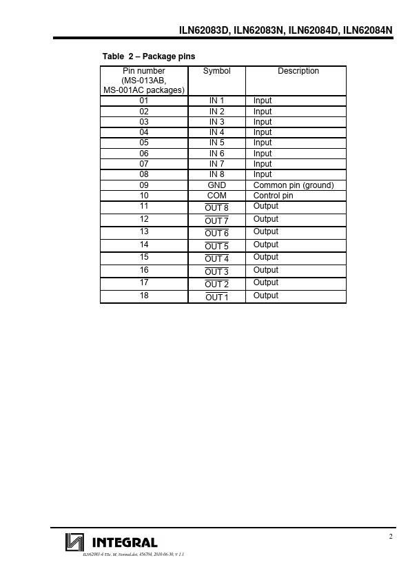
Input Input Input Input Input Input Input Input Common pin (ground) Control pin Output Output Output Output Output Output Output Output
ILN62083-4-TSe, M, Normal.dot, 456704, 2010-06-30, V 1.1
2
ILN62083D, ILN62083N, ILN62084D, ILN62084N
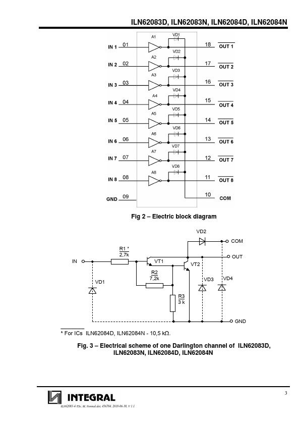
Fig 2
Electric block diagram
R1
2,7k IN
VD1
VT1
R2 7,2k
VD2
COM
OUT VT2
VD3 VD4
R3 3k
_______
For ICs ILN62084D, ILN62084N - 10,5 kΩ.
Electrical scheme of one Darlington channel of ILN62083D, ILN62083N, IL
Features
- 18
MS-001AC package
1
MS-013AB package
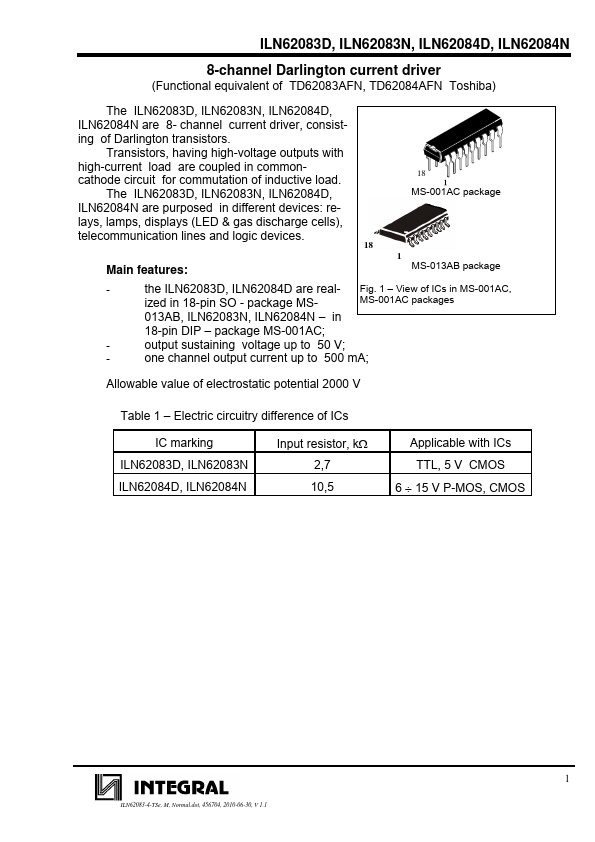
- the ILN62083D, ILN62084D are real- Fig. 1.
- View of ICs in MS-001AC,
ized in 18-pin SO - package MS-
MS-001AC packages
013AB, ILN62083N, ILN62084N.
- in
18-pin DIP.
- package MS-001AC;
- output sustaining voltage up to 50 V;
- one channel output current up to 500 mA;
Allowable value of electrostatic potential 2000 V
Table 1.
- Electric circuitry difference of ICs
IC marking ILN62083D, ILN62083N ILN62084D, ILN62084N.
 ILN62083D-Integral.pdf