Click to expand full text
isc Silicon NPN Power Transistor
DESCRIPTION ·Excellent Safe Operating Area ·Low Collector-Emitter Saturation Voltage ·100% avalanche tested ·Minimum Lot-to-Lot variations for robust device
performance and reliable operation.
APPLICATIONS ·Designed for medium-speed switching and
amplifier applications.
ABSOLUTE MAXIMUM RATINGS(Ta=25℃)
SYMBOL
PARAMETER
VALUE
UNIT
VCBO
Collector-Base Voltage
100
V
VCEO
Collector-Emitter Voltage
80
V
VEBO
Emitter-Base Voltage
7
V
IC
Collector Current-Continuous
10
A
PC
Collector Power Dissipation@TC=25℃ 150
W
TJ
Junction Temperature
-65~200 ℃
Tstg
Storage Temperature
-65~200 ℃
THERMAL CHARACTERISTICS
SYMBOL
PARAMETER
Rth j-c Thermal Resistance,Junction to Case
MAX UNIT 1.17 ℃/W
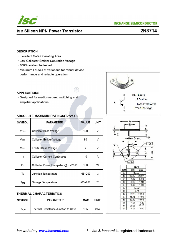
2N3714
isc website:www.iscsemi.
 2N3714 Datasheet