The following content is an automatically extracted verbatim text
from the original manufacturer datasheet and is provided for reference purposes only.
View original datasheet text
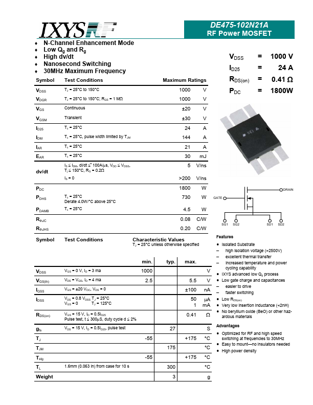
DE475-102N21A
RF Power MOSFET
♦ ♦ ♦ ♦ ♦
N-Channel Enhancement Mode Low Qg and Rg High dv/dt Nanosecond Switching 30MHz Maximum Frequency
Test Conditions
TJ = 25°C to 150°C TJ = 25°C to 150°C; RGS = 1 MΩ Continuous Transient Tc = 25°C Tc = 25°C, pulse width limited by TJM Tc = 25°C Tc = 25°C IS ≤ IDM, di/dt ≤ 100A/µs, VDD ≤ VDSS, Tj ≤ 150°C, RG = 0.2Ω IS = 0
VDSS ID25
Maximum Ratings 1000 1000 ±20 ±30 24 144 21 30 5 >200 1800 V V V V A A A mJ V/ns V/ns W W W C/W C/W
SG1 SG2 GATE
= = = =
1000 V 24 A 0.41 Ω 1800W
Symbol VDSS VDGR VGS VGSM ID25 IDM IAR EAR dv/dt PDC PDHS PDAMB RthJC RthJHS Symbol
RDS(on) PDC
DRAIN
Tc = 25°C Derate 4.0W/°C above 25°C Tc = 25°C
730 4.5 0.08 0.20
SD1
SD2
Test Conditions
Characteristic Values
Features
TJ = 25°C unless otherwise specified
min.
 DE475-102N21A Datasheet