Click to expand full text
isc Silicon NPN RF Transistor
INCHANGE Semiconductor
BFG540/X
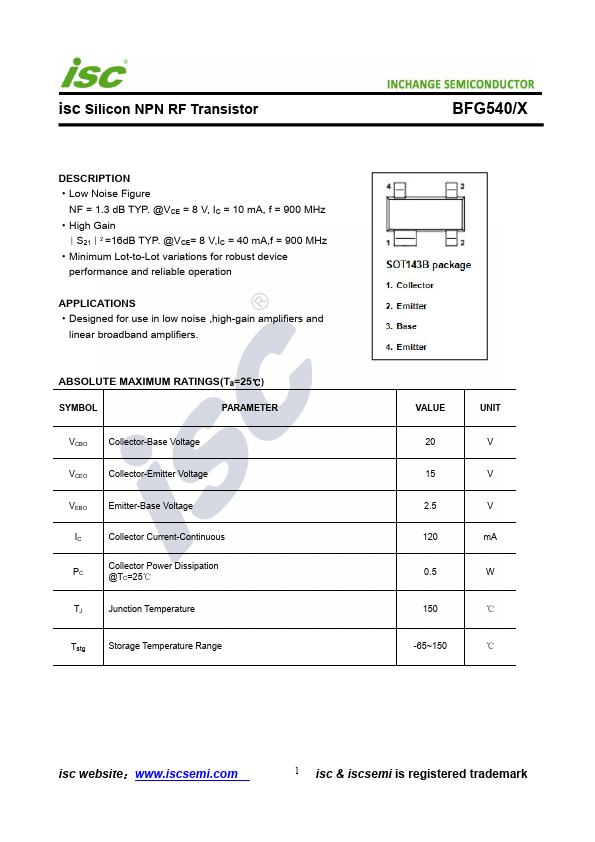
DESCRIPTION ·Low Noise Figure
NF = 1.3 dB TYP. @VCE = 8 V, IC = 10 mA, f = 900 MHz ·High Gain
︱S21︱2 =16dB TYP. @VCE= 8 V,IC = 40 mA,f = 900 MHz ·Minimum Lot-to-Lot variations for robust device
performance and reliable operation
APPLICATIONS ·Designed for use in low noise ,high-gain amplifiers and
linear broadband amplifiers.
ABSOLUTE MAXIMUM RATINGS(Ta=25℃)
SYMBOL
PARAMETER
VCBO Collector-Base Voltage
VCEO Collector-Emitter Voltage
VEBO Emitter-Base Voltage
IC
Collector Current-Continuous
PC
Collector Power Dissipation @TC=25℃
TJ
Junction Temperature
Tstg
Storage Temperature Range
VALUE 20 15 2.5 120 0.5 150
-65~150
UNIT V V V mA W ℃ ℃
isc website:www.iscsemi.
 BFG540-X Datasheet