AOD4130
FEATURES
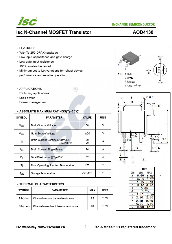
- With To-252(DPAK) package
- Low input capacitance and gate charge
- Low gate input resistance
- 100% avalanche tested
- Minimum Lot-to-Lot variations for robust device performance and reliable operation
- APPLICATIONS
- Switching applications
- Load switch
- Power management
- ABSOLUTE MAXIMUM RATINGS(Ta=25℃)
SYMBOL
PARAMETER
VALUE
VDSS
Drain-Source Voltage
VGSS ID IDM
Gate-Source Voltage
Drain Current-Continuous Tc=25℃ Tc=100℃
Drain Current-Single Pulsed
±20
30 20
Total Dissipation @TC=25℃
Tj
Max. Operating Junction Temperature
Tstg
Storage Temperature
-55~175
UNIT V V A A W ℃ ℃
- THERMAL CHARACTERISTICS
SYMBOL
PARAMETER
Rth(ch-c) Channel-to-case thermal resistance
Rth(ch-a) Channel-to-ambient thermal resistance
MAX 2.9 20
UNIT ℃/W ℃/W isc website:.iscsemi.cn...