Datasheet Details
- Part number
- SSTE32882HLB
- Manufacturer
- IDT
- File Size
- 1.22 MB
- Datasheet
- SSTE32882HLB-IDT.pdf
- Description
- 1.35V/1.5V REGISTERING CLOCK DRIVER
SSTE32882HLB Description
DATASHEET 1.35V/1.5V REGISTERING CLOCK DRIVER WITH PARITY TEST AND QUAD CHIP SELECT SSTE32882HLB .
This 28-bit 1:2, or 26-bit 1:2 and 4-bit 1:1, registering clock driver with parity is designed for 1.
SSTE32882HLB Features
* Pinout optimizes DDR3 RDIMM PCB layout
* 1-to-2 Register Outputs and 1-to-4 Clock Pair Outputs support stacked DDR3 RDIMMs
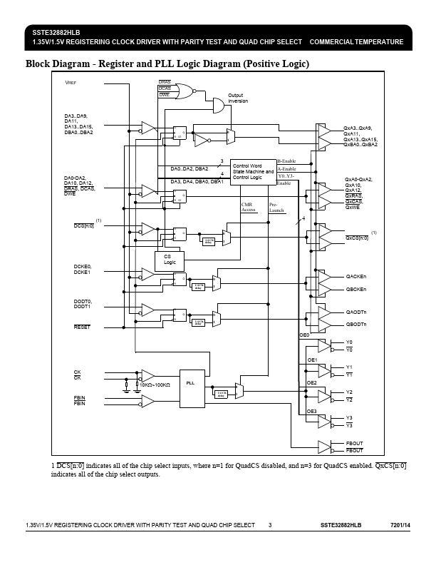
* Phase Lock Loop clock driver for buffering one differential clock pair (CK and CK) and distributing to four differential outputs
* Supports L
SSTE32882HLB Applications
* except the open-drain error (ERROUT) output. The clock outputs (Yn and Yn) and control net outputs QnCKEn, QnCSn and QnODTn are designed with a different strength and skew to compensate for different loading and equalize signal travel speed. The SSTE32882HLB has two basic modes of operation associa
📁 Related Datasheet
📌 All Tags