Datasheet Details
| Part number | IDTCSP2510D |
|---|---|
| Manufacturer | IDT |
| File Size | 91.80 KB |
| Description | 3.3V PHASE-LOCK LOOP CLOCK DRIVER |
| Datasheet |
 IDTCSP2510D_IDT.pdf IDTCSP2510D_IDT.pdf
|
| Part number | IDTCSP2510D |
|---|---|
| Manufacturer | IDT |
| File Size | 91.80 KB |
| Description | 3.3V PHASE-LOCK LOOP CLOCK DRIVER |
| Datasheet |
IDTCSP2510D_IDT.pdf
|
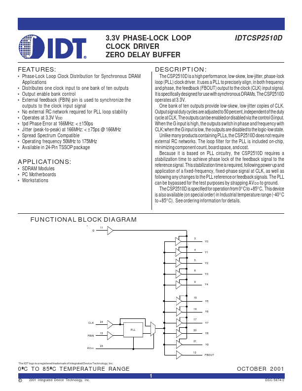
Phase-Lock Loop Clock Distribution for Synchronous DRAM Applications Distributes one clock input to one bank of ten outputs Output enable bank control External feedback (FBIN) pin is used to synchronize the outputs to the clock input signal No external RC network required for PLL loop stability Operates at 3.3V VDD tpd Phase Error at 166MHz: < ±150ps Jitter (peak-to-peak) at 166MHz: < ±75ps @ 166MHz Spread
📁 IDTCSP2510D Similar Datasheet