Datasheet Details
| Part number | 5P83905 |
|---|---|
| Manufacturer | IDT |
| File Size | 341.16 KB |
| Description | High-Performance 1.8V/2.5V/3.3V Crystal Input to LVCMOS Clock Fanout Buffer |
| Datasheet |
 5P83905 Datasheet 5P83905 Datasheet
|
|
|
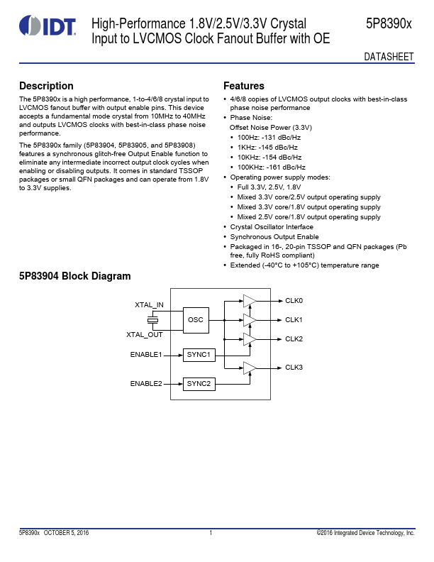
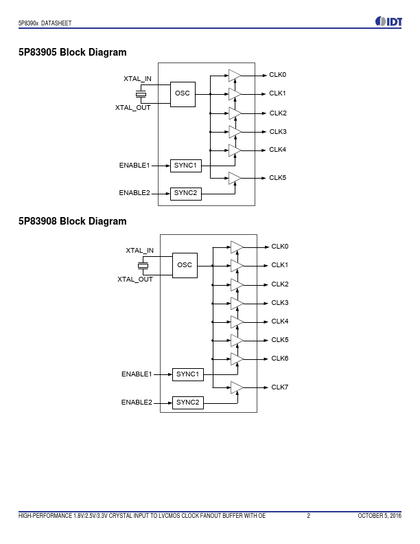
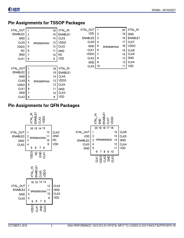
The 5P8390x is a high performance, 1-to-4/6/8 crystal input to LVCMOS fanout buffer with output enable pins.
This device accepts a fundamental mode crystal from 10MHz to 40MHz and outputs LVCMOS clocks with best-in-class phase noise performance.
| Part number | 5P83905 |
|---|---|
| Manufacturer | IDT |
| File Size | 341.16 KB |
| Description | High-Performance 1.8V/2.5V/3.3V Crystal Input to LVCMOS Clock Fanout Buffer |
| Datasheet |
5P83905 Datasheet
|
|
|
|