Datasheet Details
| Part number | CD4081B |
|---|---|
| Manufacturer | HTC KOREA |
| File Size | 157.46 KB |
| Description | CMOS Quad 2-Input AND Gates |
| Datasheet |
 CD4081B Datasheet CD4081B Datasheet
|
|
|
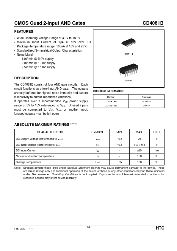
The CD4081B consist of four AND gate circuits.
Each circuit functions as a two-input AND gate.
The outputs are fully buffered for highest noise immunity and pattern insensitivity to output impedance variations.
| Part number | CD4081B |
|---|---|
| Manufacturer | HTC KOREA |
| File Size | 157.46 KB |
| Description | CMOS Quad 2-Input AND Gates |
| Datasheet |
CD4081B Datasheet
|
|
|
|