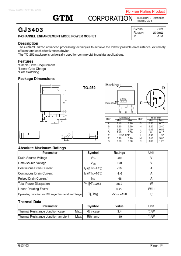
Package Dimensions TO-252
REF. A B C D E F S
Millimeter Min. Max. 6.40 6.80 5.20 5.50 6.80 7.20 2.40 3.00 2.30 REF. 0.70 0.90 0.60 0.90
REF. G H J K L M R
Millimeter Min. Max. 0.50 0.70 2.20 2.40 0.45 0.55 0 0.15 0.90 1.50 5.40 5.80 0.80 1.20
Absolute Maximum Ratings
Parameter Drain-Source Voltage Gate-Source Voltage Continuous Drain Current Continuous Drain Current Pulsed Drain Current
1
Symbol VDS VGS ID @TC=25 ID @TC=70 IDM PD @TC=25 Tj, Tstg
Ratings -30 ±20 -10 -8.6 -48 36.7 0.29 -55.
The following content is an automatically extracted verbatim text
from the original manufacturer datasheet and is provided for reference purposes only.
View original datasheet text
www.DataSheet4U.com
Pb Free Plating Product
ISSUED DATE :2005/02/25 REVISED DATE :
GJ3403
P-CHANNEL ENHANCEMENT MODE POWER MOSFET
BVDSS RDS(ON) ID
-30V 200m -10A
The GJ3403 utilized advanced processing techniques to achieve the lowest possible on-resistance, extremely efficient and cost-effectiveness device. The TO-252 package is universally used for commercial-industrial applications. *Simple Drive Requirement *Lower Gate Charge *Fast Switching
Description
Features
Package Dimensions TO-252
REF. A B C D E F S
Millimeter Min. Max. 6.40 6.80 5.20 5.50 6.80 7.20 2.40 3.00 2.30 REF. 0.70 0.90 0.60 0.90
REF. G H J K L M R
Millimeter Min. Max. 0.50 0.70 2.20 2.40 0.45 0.55 0 0.15 0.90 1.50 5.40 5.80 0.80 1.
 GJ3403 Datasheet