Download the GS8342Q10BD datasheet PDF.
This datasheet also covers the GS8342Q07BD-357 variant, as both devices belong to the same 36mb sigmaquad-ii+ burst of 2 sram family and are provided as variant models within a single manufacturer datasheet.
Description
Table
Symbol
Description
Type Comments
SA
Synchronous Address Inputs
Input
R
Synchronous Read
Input Active Low
W
Synchronous Write
Input Active Low
BW0
BW3
Synchronous Byte Writes
Input Active Low
NW0
NW1
Synchronous Nybble Writes
Input
Active Low (x8 onl
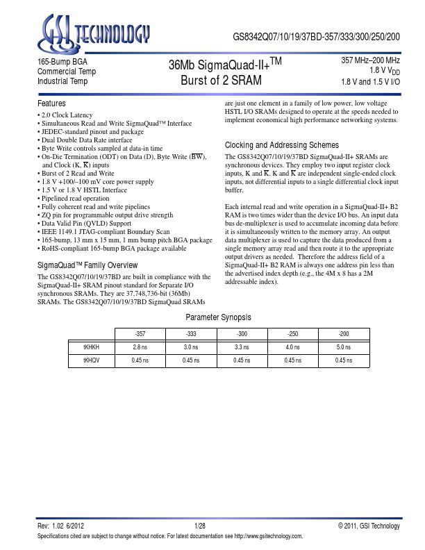
Features
- 2.0 Clock Latency.
- Simultaneous Read and Write SigmaQuad™ Interface.
- JEDEC-standard pinout and package.
- Dual Double Data Rate interface.
- Byte Write controls sampled at data-in time.
- On-Die Termination (ODT) on Data (D), Byte Write (BW),
and Clock (K, K) inputs.
- Burst of 2 Read and Write.
- 1.8 V +100/.
- 100 mV core power supply.
- 1.5 V or 1.8 V HSTL Interface.
- Pipelined read operation.
- Fully co.
 GS8342Q10BD Datasheet