Description
GS8342D07/10/19/37BD-450/400/350/333/300 165-Bump BGA Commercial Temp Industrial Temp 36Mb SigmaQuad-II+TM Burst of 4 SRAM 450 MHz *300 MHz .
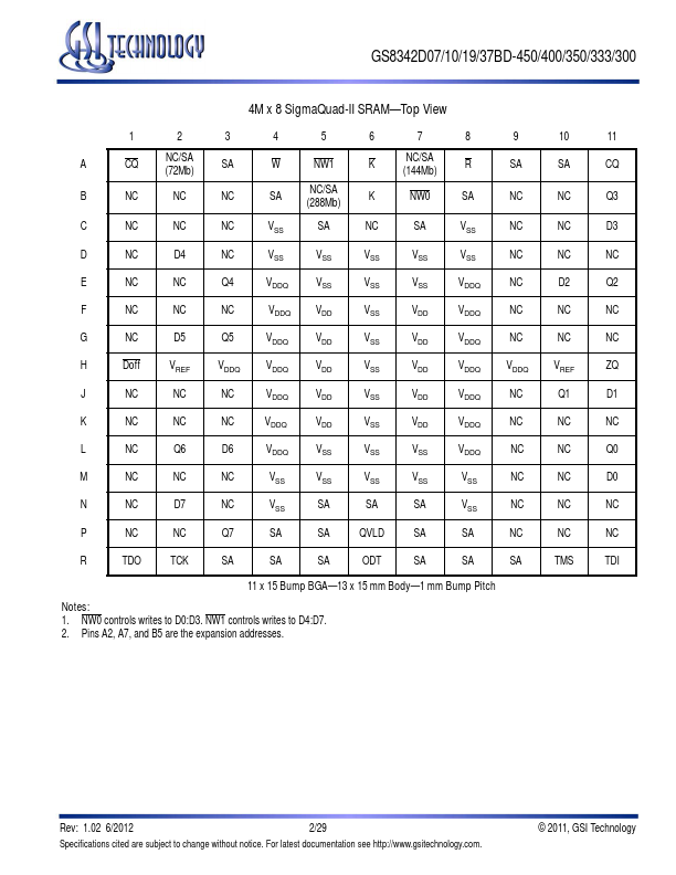
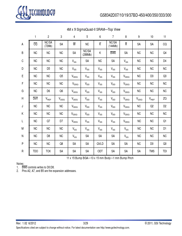
Table
Symbol
Description
Type Comments
SA
Synchronous Address Inputs
Input.
R
Synchronous Read
Input Active Low
W
Synchronous Writ.
Features
* 2.0 Clock Latency
* Simultaneous Read and Write SigmaQuad™ Interface
* JEDEC-standard pinout and package
* Dual Double Data Rate interface
* Byte Write controls sampled at data-in time
* Burst of 4 Read and Write
* On-Die Termination (ODT) on
Applications
* where alternating reads and writes are needed. Therefore, the SigmaQuad-II+ SRAM interface and truth table are optimized for alternating reads and writes. Separate I/O SRAMs are unpopular in applications where multiple reads or multiple writes are needed because burst read or write transfers from Se