Datasheet4U Logo Datasheet4U.com

GS81302TT06E - 144Mb SigmaDDR-II+ Burst of 2 SRAM

Download the GS81302TT06E datasheet PDF (GS81302TT06E-500 included). The manufacturer datasheet provides complete specifications, pinout details, electrical characteristics, and typical applications for 144mb sigmaddr-ii+ burst of 2 sram.

Features

  • 2.5 Clock Latency.
  • Simultaneous Read and Write SigmaDDRTM Interface.
  • JEDEC-standard pinout and package.
  • Double Data Rate interface.
  • Byte Write controls sampled at data-in time.
  • Burst of 2 Read and Write.
  • Dual-Range On-Die Termination (ODT) on Data (D), Byte Write (BW), and Clock (K, K) inputs.
  • 1.8 V +100/.
  • 100 mV core power supply.
  • 1.5 V or 1.8 V HSTL Interface.
  • Pipelined read operation.
  • Fu.

📥 Download Datasheet

Note: The manufacturer provides a single datasheet file (GS81302TT06E-500-GSITechnology.pdf) that lists specifications for multiple related part numbers.

Datasheet Details

Part number GS81302TT06E
Manufacturer GSI Technology
File Size 227.52 KB
Description 144Mb SigmaDDR-II+ Burst of 2 SRAM
Datasheet download datasheet GS81302TT06E Datasheet
Other Datasheets by GSI Technology

Full PDF Text Transcription

Click to expand full text
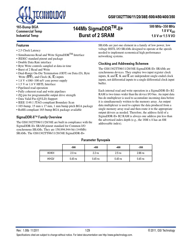
GS81302TT06/11/20/38E-500/450/400/350 165-Bump BGA Commercial Temp Industrial Temp 144Mb SigmaDDRTM-II+ Burst of 2 SRAM 500 MHz–350 MHz 1.8 V VDD 1.8 V or 1.5 V I/O Features • 2.5 Clock Latency • Simultaneous Read and Write SigmaDDRTM Interface • JEDEC-standard pinout and package • Double Data Rate interface • Byte Write controls sampled at data-in time • Burst of 2 Read and Write • Dual-Range On-Die Termination (ODT) on Data (D), Byte Write (BW), and Clock (K, K) inputs • 1.8 V +100/–100 mV core power supply • 1.5 V or 1.8 V HSTL Interface • Pipelined read operation • Fully coherent read and write pipelines • ZQ pin for programmable output drive strength • Data Valid Pin (QVLD) Support • IEEE 1149.
Published: |