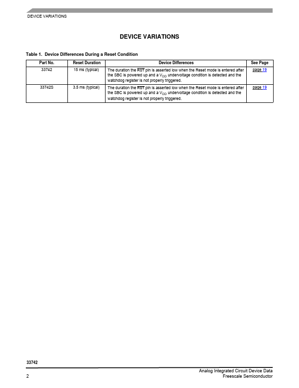
Description
of each pin can be found in the Functional Pin description section beginning on page 22.
9 20
23 10 11 12 13 14
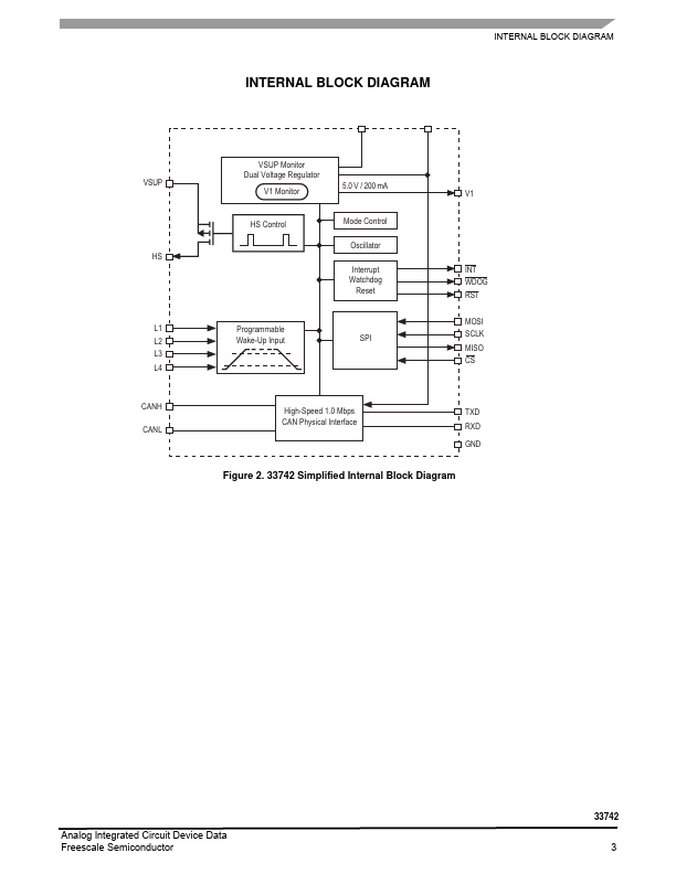
17 18 19 24 25 26 27 28 Pin Name RXD TXD VDD RST INT GND V2 V2CTRL VSUP HS L0- L3 CANH CANL SCLK MISO MOSI
CS WDOG
Formal Name Receive Data Transmit Data Voltage Digital Drain Reset Output (Active LOW) Interrupt Output (Active LOW) Ground Voltage Source 2 Voltage Source 2 Control Voltage Supply High-Side Output Level 0 - 3 Inputs CAN High Out
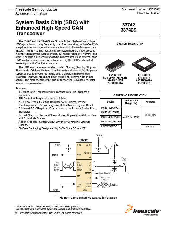
Features
- 1.0 Mbps CAN Transceiver Bus Interface with Bus Diagnostic Capability.
- SPI Control at Frequencies up to 4.0 Mhz.
- 5.0 V Low Dropout Voltage Regulator with Current Limiting, Overtemperature Pre-Warning, and Output Monitoring and Reset.
- A Second 5.0 V Regulator Capability using an External Series Pass Transistor.
- Normal, Standby, Stop, and Sleep Modes of Operation with Low Sleep and Stop Mode Current.
- A High-Side (HS) Switch Output Driver for C.
 MCZ33742S Datasheet