Datasheet4U Logo Datasheet4U.com

PF5103 N-Channel Switch

PF5103 Description

PF5103 N-Channel Switch October 2006 PF5103 N-Channel Switch .

PF5103 Features

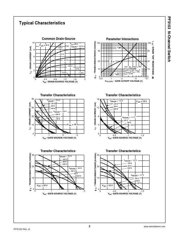
* This device is designed for low level analog switching sample and hold circuits and chopper stabilized amplifiers.
* Sourced from process 51. tm TO-92 1 2 3 Marking : PF5103 1. Drain 2. Source 3. Gate Absolute Maximum Ratings
* Symbol VDG VGS IGF TJ, TSTG Drain-Gate Voltag

PF5103 Applications

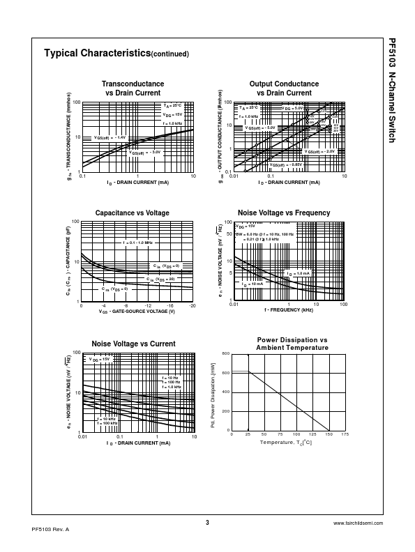
* involving pulsed or low duty cycle operations. Thermal Characteristics
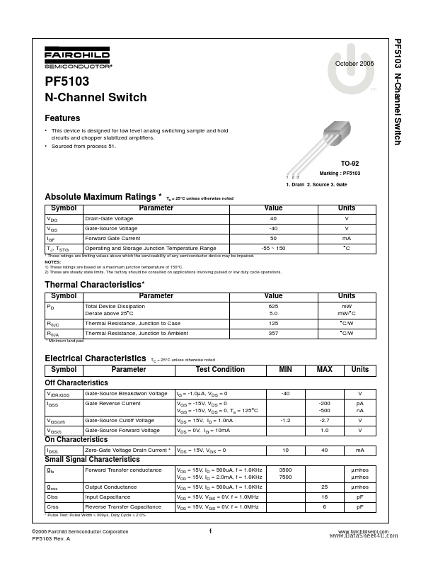
* Symbol PD RθJC RθJA
* Minimum land pad. Parameter Total Device Dissipation Derate above 25°C Thermal Resistance, Junction to Case Thermal Resistance, Junction to Ambient Value 625 5.0 125 357 Units mW mW/°C °C/W °C/W

📥 Download Datasheet

Preview of PF5103 PDF
datasheet Preview Page 2 datasheet Preview Page 3

📁 Related Datasheet

  • PF5101 - N-Channel JFET (National Semiconductor)
  • PF5000 - PRESS-FIT DIODE (WON-TOP)
  • PF5001 - PRESS-FIT DIODE (WON-TOP)
  • PF5002 - PRESS-FIT DIODE (WON-TOP)
  • PF5003 - PRESS-FIT DIODE (WON-TOP)
  • PF5004 - PRESS-FIT DIODE (WON-TOP)
  • PF5005 - PRESS-FIT DIODE (WON-TOP)
  • PF5006 - PRESS-FIT DIODE (WON-TOP)

📌 All Tags

Fairchild Semiconductor PF5103-like datasheet