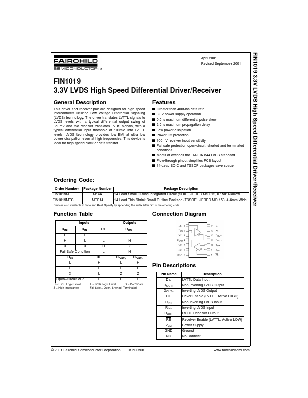
Datasheet4U Logo Datasheet4U.com

FIN1019 - 3.3V LVDS High Speed Differential Driver/Receiver

Description

This driver and receiver pair are designed for high speed interconnects utilizing Low Voltage Differential Signaling (LVDS) technology.

Features

  • s Greater than 400Mbs data rate s 3.3V power supply operation s 0.5ns maximum differential pulse skew s 2.5ns maximum propagation delay s Low power dissipation s Power-Off protection s 100mV receiver input sensitivity s Fail safe protection open-circuit, shorted and terminated conditions s Meets or exceeds the TIA/EIA-644 LVDS standard s Flow-through pinout simplifies PCB layout s 14-Lead SOIC and TSSOP packages save space Ordering Code: Order Number FIN1019M FIN1019MTC Package Number M14A MTC1.

📥 Download Datasheet

Full PDF Text Transcription (Reference)

The following content is an automatically extracted verbatim text from the original manufacturer datasheet and is provided for reference purposes only.

View original datasheet text
FIN1019 3.3V LVDS High Speed Differential Driver/Receiver April 2001 Revised September 2001 FIN1019 3.3V LVDS High Speed Differential Driver/Receiver General Description This driver and receiver pair are designed for high speed interconnects utilizing Low Voltage Differential Signaling (LVDS) technology. The driver translates LVTTL signals to LVDS levels with a typical differential output swing of 350mV and the receiver translates LVDS signals, with a typical differential input threshold of 100mV, into LVTTL levels. LVDS technology provides low EMI at ultra low power dissipation even at high frequencies. This device is ideal for high speed clock or data transfer. Features s Greater than 400Mbs data rate s 3.3V power supply operation s 0.5ns maximum differential pulse skew s 2.
Published: |