Datasheet Details
| Part number | 74VCX16827 |
|---|---|
| Manufacturer | Fairchild (onsemi) |
| File Size | 133.15 KB |
| Description | Low Voltage 20-Bit Buffer/Line Driver |
| Datasheet |
 74VCX16827 Datasheet 74VCX16827 Datasheet
|
|
|
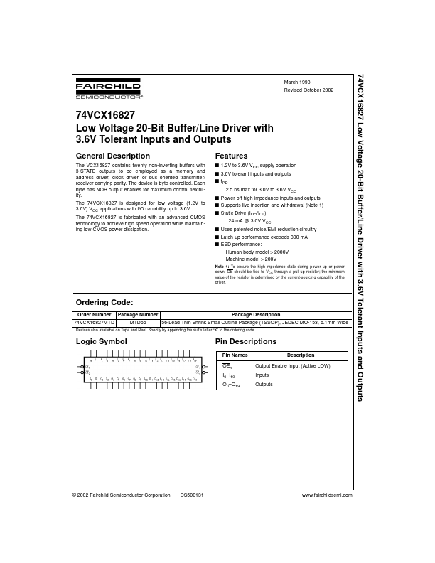
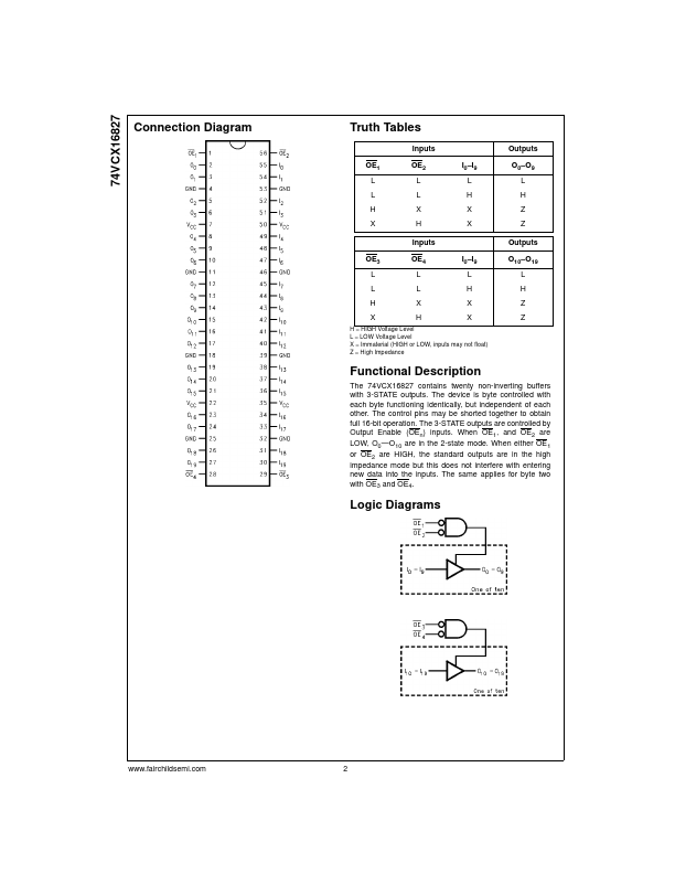
The VCX16827 contains twenty non-inverting buffers with 3-STATE outputs to be employed as a memory and address driver, clock driver, or bus oriented transmitter/ receiver carrying parity.
The device is byte controlled.
Each byte has NOR output enables for maximum control flexibility.
| Part number | 74VCX16827 |
|---|---|
| Manufacturer | Fairchild (onsemi) |
| File Size | 133.15 KB |
| Description | Low Voltage 20-Bit Buffer/Line Driver |
| Datasheet |
74VCX16827 Datasheet
|
|
|
|
| Part Number | Description | Manufacturer |
|---|---|---|
| 74VCX162244 | LOW VOLTAGE CMOS 16-BIT BUS BUFFER | ST Microelectronics |
| 74VCX16240 | LOW VOLTAGE CMOS 16-BIT BUS BUFFER | STMicroelectronics |
| 74VCX16240 | Low-Voltage 1.8/2.5/3.3V 16-Bit Buffer | ON Semiconductor |
| 74VCX16244 | Low-Voltage 1.8V/2.5V/3.3V 16-Bit Buffer | ON Semiconductor |
| 74VCX16245 | Low-Voltage 1.8/2.5/3.3V 16-Bit Transceiver | ON Semiconductor |
| Part Number | Description |
|---|---|
| 74VCX16821 | Low Voltage 20-Bit D-Type Flip-Flops |
| 74VCX16835 | Low Voltage 18-Bit Universal Bus Driver |
| 74VCX16838 | Low Voltage 16-Bit Selectable Register/Buffer |
| 74VCX16839 | Low Voltage 20-Bit Selectable Register/Buffer |
| 74VCX16841 | Low Voltage 20-Bit Transparent Latch |
The following content is an automatically extracted verbatim text from the original manufacturer datasheet and is provided for reference purposes only.