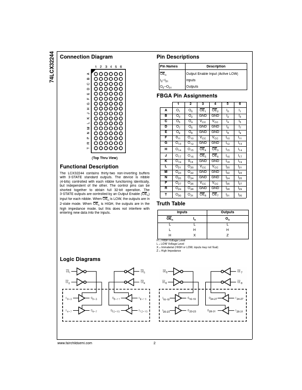
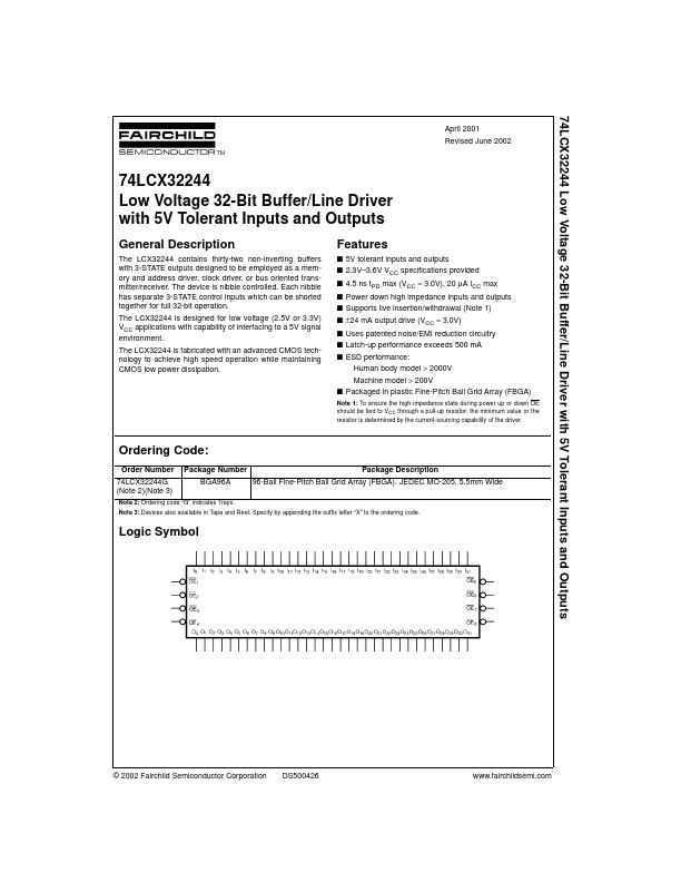
Datasheet4U Logo Datasheet4U.com

74LCX32244 - Low Voltage 32-Bit Buffer/Line Driver

Description

The LCX32244 contains thirty-two non-inverting buffers with 3-STATE outputs designed to be employed as a memory and address driver, clock driver, or bus oriented transmitter/receiver.

The device is nibble controlled.

Features

  • s 5V tolerant inputs and outputs s 2.3V.
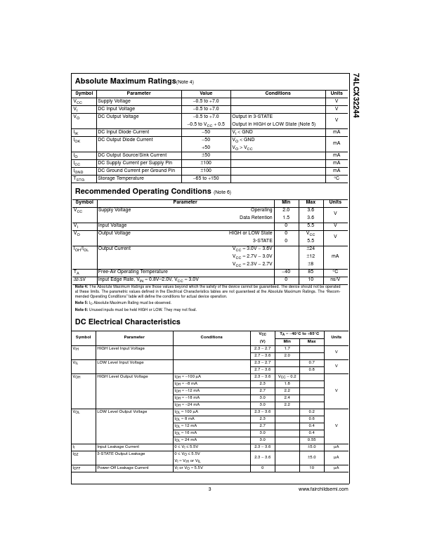
  • 3.6V VCC specifications provided s 4.5 ns tPD max (VCC = 3.0V), 20 µA ICC max s Power down high impedance inputs and outputs s Supports live insertion/withdrawal (Note 1) s ±24 mA output drive (VCC = 3.0V) s Uses patented noise/EMI reduction circuitry s Latch-up performance exceeds 500 mA s ESD performance: Human body model > 2000V Machine model > 200V s Packaged in plastic Fine-Pitch Ball Grid Array (FBGA) Note 1: To ensure the high-impedance stat.

📥 Download Datasheet

Full PDF Text Transcription (Reference)

The following content is an automatically extracted verbatim text from the original manufacturer datasheet and is provided for reference purposes only.

View original datasheet text
74LCX32244 Low Voltage 32-Bit Buffer/Line Driver with 5V Tolerant Inputs and Outputs April 2001 Revised June 2002 74LCX32244 Low Voltage 32-Bit Buffer/Line Driver with 5V Tolerant Inputs and Outputs General Description The LCX32244 contains thirty-two non-inverting buffers with 3-STATE outputs designed to be employed as a memory and address driver, clock driver, or bus oriented transmitter/receiver. The device is nibble controlled. Each nibble has separate 3-STATE control inputs which can be shorted together for full 32-bit operation. The LCX32244 is designed for low voltage (2.5V or 3.3V) VCC applications with capability of interfacing to a 5V signal environment.