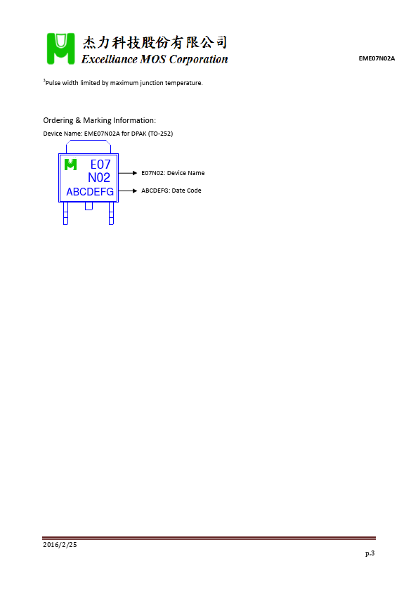
Click to expand full text
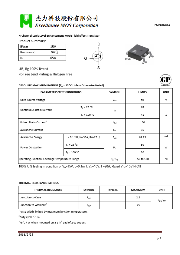
EME07N02A
N‐Channel Logic Level Enhancement Mode Field Effect Transistor
Product Summary:
BVDSS
15V
D
RDSON (MAX.)
7mΩ
ID
65A
G
UIS, Rg 100% Tested
S
Pb‐Free Lead Plating & Halogen Free
ABSOLUTE MAXIMUM RATINGS (TA = 25 °C Unless Otherwise Noted) PARAMETERS/TEST CONDITIONS
SYMBOL
LIMITS
Gate‐Source Voltage
Continuous Drain Current Pulsed Drain Current1
TC = 25 °C TC = 100 °C
Avalanche Current
Avalanche Energy
L = 0.1mH, ID=35A, RG=25Ω
Power Dissipation
TC = 25 °C TC = 100 °C
Operating Junction & Storage Temperature Range
VGS ID
IDM IAS EAS PD Tj, Tstg
±8 65 41 160 35 61.25 50 20 ‐55 to 150
100% UIS testing in condition of VD=15V, L=0.
 EME07N02A Datasheet