The following content is an automatically extracted verbatim text
from the original manufacturer datasheet and is provided for reference purposes only.
View original datasheet text
ESMT
M13S64164A (2Y)
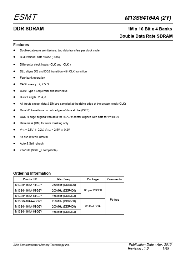
DDR SDRAM
1M x 16 Bit x 4 Banks Double Data Rate SDRAM
Features
z Double-data-rate architecture, two data transfers per clock cycle
z Bi-directional data strobe (DQS)
z Differential clock inputs (CLK and CLK ) z DLL aligns DQ and DQS transition with CLK transition z Four bank operation z CAS Latency : 2, 2.5, 3 z Burst Type : Sequential and Interleave z Burst Length : 2, 4, 8 z All inputs except data & DM are sampled at the rising edge of the system clock (CLK) z Data I/O transitions on both edges of data strobe (DQS) z DQS is edge-aligned with data for READs; center-aligned with data for WRITEs z Data mask (DM) for write masking only z VDD = 2.5V ± 0.2V, VDDQ = 2.5V ± 0.2V z 15.6us refresh interval z Auto & Self refresh z 2.
 M13S64164A-6TG2Y Datasheet