Datasheet Details
| Part number | 74LVC2G125 |
|---|---|
| Manufacturer | Diodes Incorporated |
| File Size | 388.49 KB |
| Description | DUAL BUFFER GATE |
| Datasheet |
 74LVC2G125 Datasheet 74LVC2G125 Datasheet
|
|
|
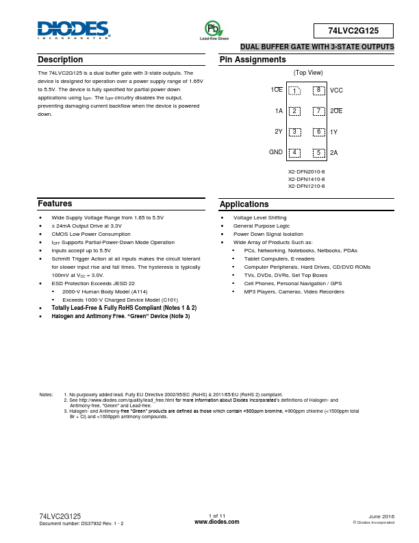
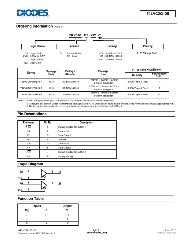
The 74LVC2G125 is a dual buffer gate with 3-state outputs.
The device is designed for operation over a power supply range of 1.65V to 5.5V.
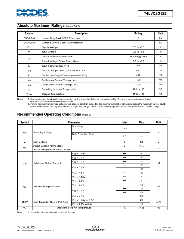
The device is fully specified for partial power down applications using IOFF.
| Part number | 74LVC2G125 |
|---|---|
| Manufacturer | Diodes Incorporated |
| File Size | 388.49 KB |
| Description | DUAL BUFFER GATE |
| Datasheet |
74LVC2G125 Datasheet
|
|
|
|
| Part Number | Description | Manufacturer |
|---|---|---|
| 74LVC2G125 | Dual bus buffer/line driver | NXP |
| 74LVC2G125 | Dual bus buffer/line driver | nexperia |
| 74LVC2G125-Q100 | Dual bus buffer/line driver | NXP |
| 74LVC2G125-Q100 | Dual bus buffer/line driver | nexperia |
| 74LVC2G126 | Dual bus buffer/line driver | NXP |
| Part Number | Description |
|---|---|
| 74LVC2G126 | DUAL BUFFER GATE |
| 74LVC2G14 | DUAL SCHMITT TRIGGER INVERTERS |
| 74LVC2G17 | DUAL SCHMITT TRIGGER BUFFERS |
| 74LVC2G00 | DUAL 2-INPUT NAND GATE |
| 74LVC2G02 | DUAL 2-INPUT NOR GATE |
The following content is an automatically extracted verbatim text from the original manufacturer datasheet and is provided for reference purposes only.