The following content is an automatically extracted verbatim text
from the original manufacturer datasheet and is provided for reference purposes only.
View original datasheet text
AP9060
OVERVOLTAGE CLAMP
Description
AP9060 is designed to protect the latest generation of PMICs for portable applications such as Smartphones, UMPCs and others that utilize battery power.
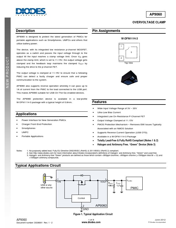
Pin Assignments
W-DFN1114-3
1
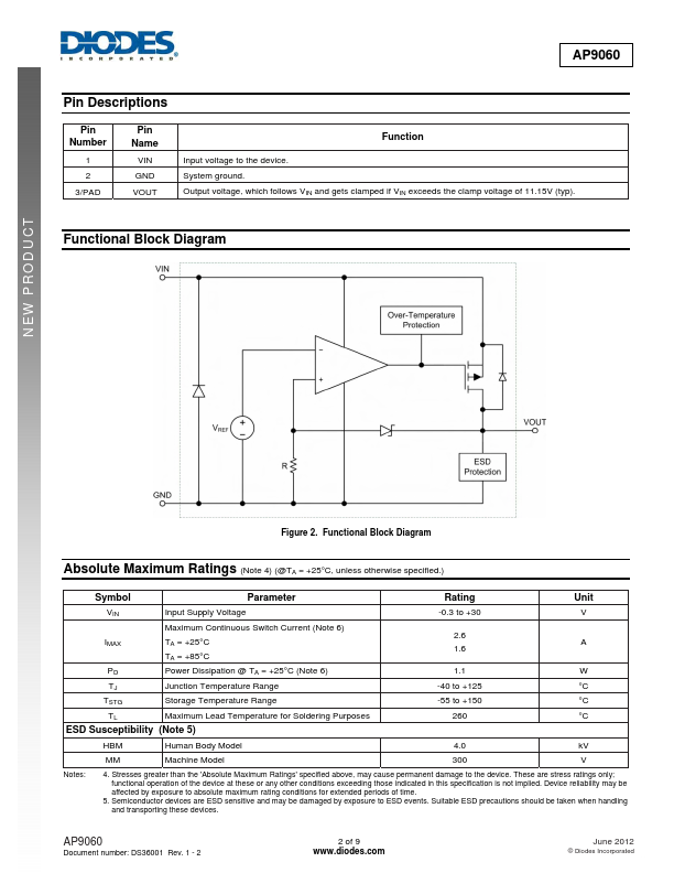
The device, with its integrated low resistance p-channel MOSFET,
NEW PRODUCT
operates as a switch and passes the input voltage through to the output till the input reaches a clamp voltage limit. Once VIN goes above the clamp limit, which is set to 11.15V, the output voltage gets clamped and the feedback loop maintains the clamped VOUT by reducing the drive to the p-channel FET. The output voltage is clamped at 11.15V to ensure that a following PMIC can detect a faulty charger and ensure safe and proper communication to the system.
 AP9060 Datasheet