Datasheet Details
| Part number | C5002 |
|---|---|
| Manufacturer | Cypress |
| File Size | 122.82 KB |
| Description | Low Skew Multiple Frequency PCI Clock Generator |
| Datasheet |
 C5002-Cypress.pdf C5002-Cypress.pdf
|
| Part number | C5002 |
|---|---|
| Manufacturer | Cypress |
| File Size | 122.82 KB |
| Description | Low Skew Multiple Frequency PCI Clock Generator |
| Datasheet |
C5002-Cypress.pdf
|
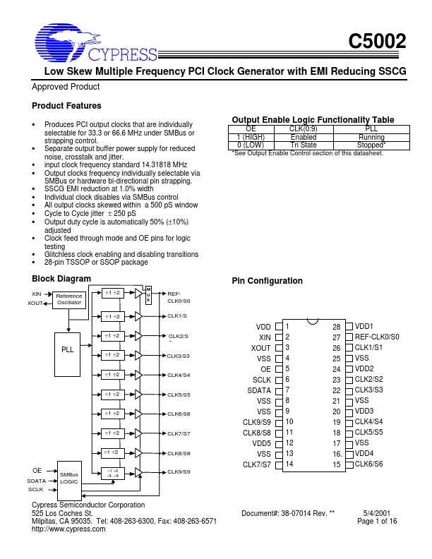
Pin Number 2 Pin Name XIN 3 XOUT 1 VDDA 5 12, 16, 20, 24, 28 6 7 27 26 23 22 19 18 15 14 11 10 4, 8, 9, 13, 17, 21, 25 1 28 24 20 16 12 OE VDD SDATA SCLK REFCLK0/S0 CLK1/S1 CLK2/S2 CLK3/S3 CLK4/S4 CLK5/S5 CLK6/S6 CLK7/S7 CLK8/S8 CLK9/S9 VSS VDD VDD1 VDD2 VDD3 VDD4 VDD5 PWR VDDA VDDA - VDDA VDDA VDD1 VDD1 VDD2 VDD2 VDD3 VDD3 VDD4 VDD4 VDD5 VDD5 - - I/O I O PWR I PWR I/O O O Description This pin is the connection point for the devices Loop reference frequency.This may be either a CMOS 3.3
📁 C5002 Similar Datasheet