Datasheet Details
| Part number | GVT7C1357A |
|---|---|
| Manufacturer | Cypress (Infineon) |
| File Size | 802.47 KB |
| Description | 256K x 36 / 512K x 18 Flow Thru SRAM |
| Datasheet |
 GVT7C1357A Datasheet GVT7C1357A Datasheet
|
|
|
Download the GVT7C1357A datasheet PDF. This datasheet also covers the GVT71256ZB36 variant, as both devices belong to the same 256k x 36 / 512k x 18 flow thru sram family and are provided as variant models within a single manufacturer datasheet.
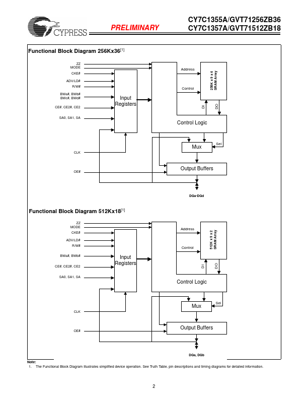
The CY7C1355A/GVT71256ZB36 and CY7C1357A/ GVT71512ZB18 SRAMs are designed to eliminate dead cycles when transitions from READ to WRITE or vice versa.
These SRAMs are optimized for 100 percent bus utilization and achieves Zero Bus Latency (ZBL)/No Bus Latency (NoBL).
| Part number | GVT7C1357A |
|---|---|
| Manufacturer | Cypress (Infineon) |
| File Size | 802.47 KB |
| Description | 256K x 36 / 512K x 18 Flow Thru SRAM |
| Datasheet |
GVT7C1357A Datasheet
|
|
|
|
| Part Number | Description | Manufacturer |
|---|
| Part Number | Description |
|---|---|
| GVT7C1354A | 256Kx36/512Kx18 Pipelined SRAM |
| GVT7C1355A | 256K x 36 / 512K x 18 Flow Thru SRAM |
| GVT7C1356A | 256Kx36/512Kx18 Pipelined SRAM |
| GVT7C1359A | 256K X 18 Synchronous-pipelined Cache Tag RAM |
| GVT7C1325A | 256K x 18 Synchronous Flow Through Burst SRAM |