Description
1]
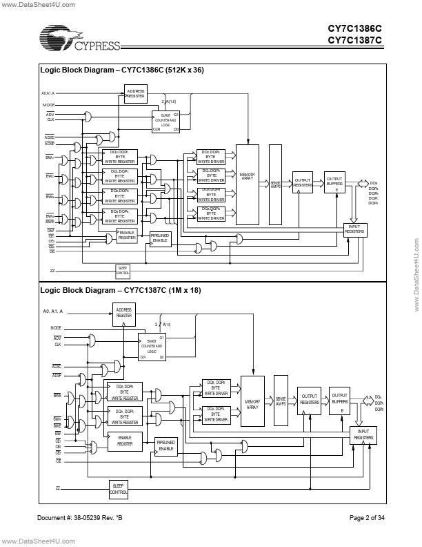
The CY7C1386C/CY7C1387C SRAM integrates 524,288 x 36 and 1048,576 x 18 SRAM cells with advanced synchronous peripheral circuitry and a two-bit counter for internal burst operation.All synchronous inputs are gated by registers controlled by a positive-edge-triggered Clock Input (CLK).The synchronous inputs include all addresses, all data inputs, address-pipelining Chip Enable (CE1), depth-expansion Chip Enables (CE2 and CE3[2]), Burst Control inputs (ADSC, ADSP, and ADV), Write Enables (BWX,
Features
- Supports bus operation up to 250 MHz.
- Available speed grades are 250, 225, 200 and 167 MHz.
- Registered inputs and outputs for pipelined operation.
- Optimal for performance (Double-Cycle deselect).
- Depth expansion without wait state.
- 3.3V.
- 5% and +10% core power supply (VDD).
- 2.5V / 3.3V I/O operation.
- Fast clock-to-output times.
- 2.6 ns (for 250-MHz device).
- 2.8 ns (for 225-MHz device).
- 3.0.
 CY7C1386C_CypressSemiconductor.pdf