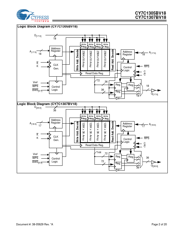
Separate independent Read and Write data ports
Supports concurrent transactions
167-MHz Clock for high bandwidth
2.5 ns Clock-to-Valid access time
4-Word Burst for reducing the address bus frequency
Double Data Rate (DDR) interfaces on bot
The following content is an automatically extracted verbatim text
from the original manufacturer datasheet and is provided for reference purposes only.
View original datasheet text
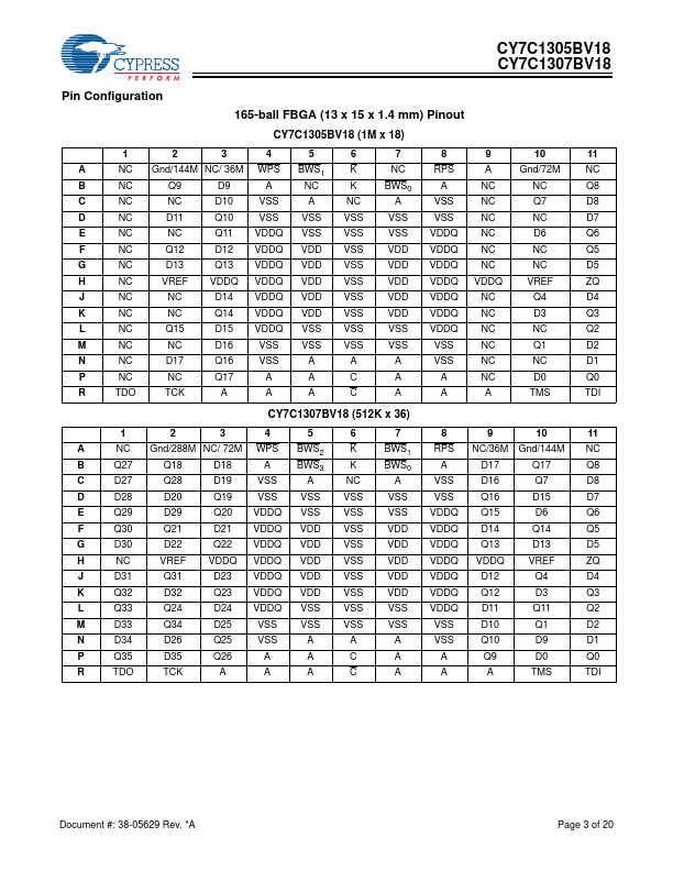
CY7C1305BV18 CY7C1307BV18
18-Mbit Burst of 4 Pipelined SRAM with QDR™ Architecture
Features
Functional Description
• Separate independent Read and Write data ports — Supports concurrent transactions
• 167-MHz Clock for high bandwidth — 2.5 ns Clock-to-Valid access time
• 4-Word Burst for reducing the address bus frequency • Double Data Rate (DDR) interfaces on both Read & Write
Ports (data transferred at 333 MHz) @167 MHz • Two input clocks (K and K) for precise DDR timing
— SRAM uses rising edges only • Two input clocks for output data (C and C) to minimize
clock-skew and flight-time mismatches. • Single multiplexed address input bus latches address
inputs for both Read and Write ports • Separate Port Selects for depth expansion • Synchronous internally self-timed writes • 1.
 CY7C1305BV18 Datasheet