Click to expand full text
www.DataSheet4U.com
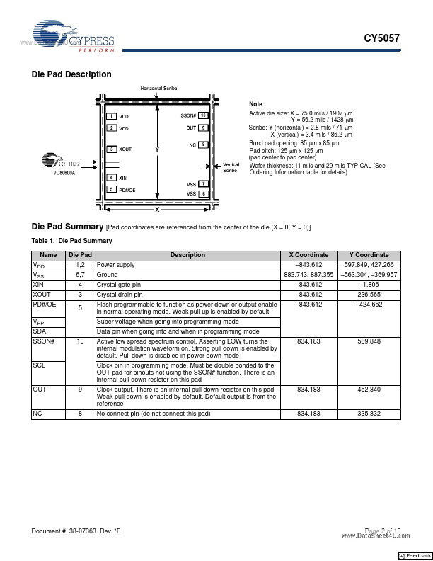
CY5057
High-Frequency Flash Programmable PLL Die with Spread Spectrum
Features
■ ■ ■ ■ ■ ■ ■ ■
Benefits
■
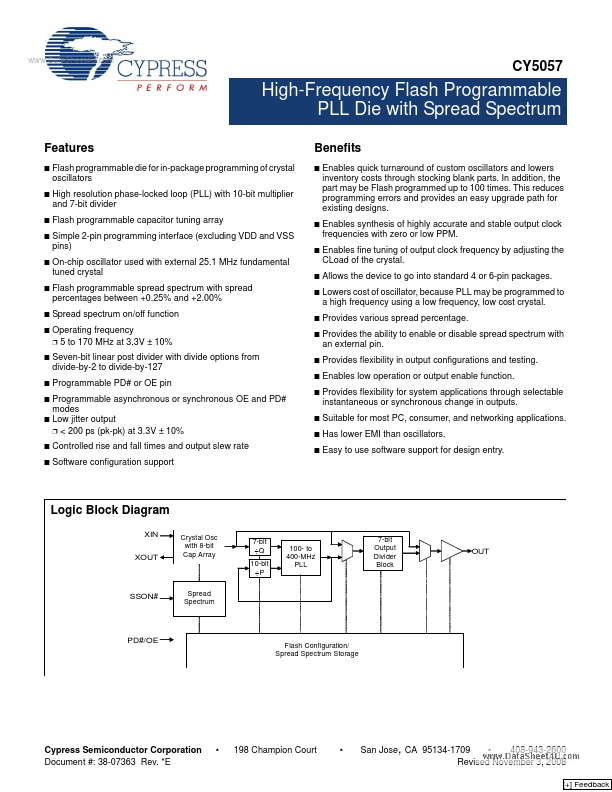
Flash programmable die for in-package programming of crystal oscillators High resolution phase-locked loop (PLL) with 10-bit multiplier and 7-bit divider Flash programmable capacitor tuning array Simple 2-pin programming interface (excluding VDD and VSS pins) On-chip oscillator used with external 25.1 MHz fundamental tuned crystal Flash programmable spread spectrum with spread percentages between +0.25% and +2.00% Spread spectrum on/off function Operating frequency ❐ 5 to 170 MHz at 3.
 CY5057 Datasheet