Datasheet4U Logo Datasheet4U.com

CY28351 Differential Clock Buffer/Driver

CY28351 Description

CY28351 Differential Clock Buffer/Driver DDR400- and DDR333-Compliant .
This PLL clock buffer is designed for 2.

CY28351 Features

* Supports 333-MHz and 400-MHz DDR SDRAM
* 60-
* 200-MHz operating frequency

CY28351 Applications

* Distributes one clock input to ten differential outputs
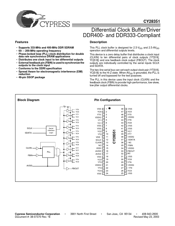
* External feedback pin (FBIN) is used to synchronize the outputs to the clock input
* Conforms to the DDRI specification
* Spread Aware for electromagnetic interference (EMI) reduction
* 48-pin SSOP pa

📥 Download Datasheet

Preview of CY28351 PDF
datasheet Preview Page 2 datasheet Preview Page 3

Datasheet Details

Part number
CY28351
Manufacturer
Cypress Semiconductor
File Size
71.38 KB
Datasheet
CY28351-CypressSemiconductor.pdf
Description
Differential Clock Buffer/Driver

📁 Related Datasheet

  • CY28354-400 - 210MHz 24 Output Buffer (Silicon Laboratories)
  • CY28322-2 - 133 Mhz Spread Spectrum Clock Synthesizer with Differential CPU Outputs (Cypress)
  • CY28341 - Universal Single-Chip Clock Solution (SpectraLinear)
  • CY28346-2 - Clock Synthesizer (Silicon Laboratories)
  • CY28349 - FTG (SpectraLinear)
  • CY28378 - FTG for Pentium 4 and Intel 845 Series Chipset (Silicon Laboratories)
  • CY28400 - 100MHz Differential Buffer (Silicon Laboratories)
  • CY28400-2 - 100MHz Differential Buffer (Silicon Laboratories)

📌 All Tags

Cypress Semiconductor CY28351-like datasheet