Click to expand full text
CES2306
N-Channel Enhancement Mode Field Effect Transistor
FEATURES
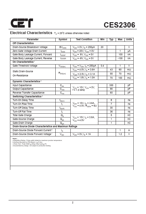
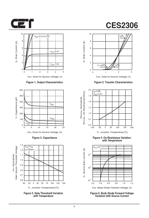
20V, 3.6A, RDS(ON) = 60mΩ @VGS = 4.5V. RDS(ON) = 70mΩ @VGS = 2.5V. RDS(ON) = 100mΩ @VGS = 1.8V.
High dense cell design for extremely low RDS(ON). Lead-free plating ; RoHS compliant. Rugged and reliable. SOT-23 package.
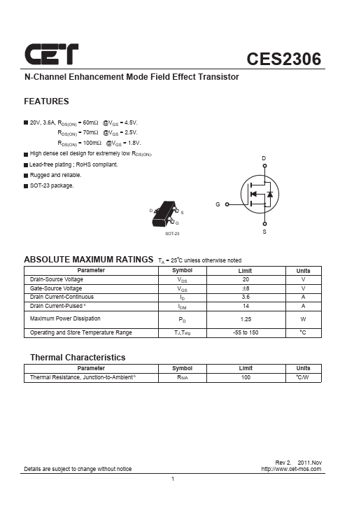
DS G
SOT-23
G
D S
ABSOLUTE MAXIMUM RATINGS TA = 25 C unless otherwise noted
Parameter
Symbol
Limit
Drain-Source Voltage Gate-Source Voltage
VDS 20
VGS ±8
Drain Current-Continuous Drain Current-Pulsed a
ID 3.6 IDM 14
Maximum Power Dissipation
PD 1.25
Operating and Store Temperature Range
TJ,Tstg
-55 to 150
Thermal Characteristics
Parameter Thermal Resistance, Junction-to-Ambient b
Symbol RθJA
Limit 100
Units V V A A W C
Units C/W
Details are subject to change without notice
1
Rev 2.
 CES2306 Datasheet