Datasheet4U Logo Datasheet4U.com

ADV3203 - 32 X 16 Buffered Analog Crosspoint Switch

This page provides the datasheet information for the ADV3203, a member of the ADV3202 32 X 16 Buffered Analog Crosspoint Switch family.

Description

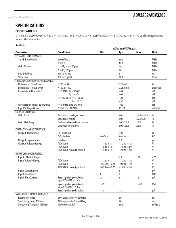
The ADV3202/ADV3203 are 32 × 16 analog crosspoint switch matrices.

They feature a selectable sync-tip clamp input for ac-coupled applications and a 2:1 on-screen display (OSD) insertion mux.

48 dB of crosstalk and 80 dB isolation at 5 MHz, the ADV3202/ADV3203 are useful in man
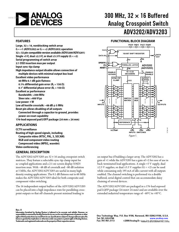
Features

  • Large, 32 × 16, nonblocking switch array G = +1 (ADV3202) or G = +2 (ADV3203) operation 32 × 32 pin-compatible version available (ADV3200/ADV3201) Single +5 V, dual ±2.5 V, or dual ±3.3 V supply (G = +2) Serial programming of switch array 2:1 OSD insertion mux per output Input sync-tip clamp High impedance output disable allows connection of multiple devices with minimal output bus load Excellent video performance 60 MHz 0.1 dB gain flatness 0.1% differential gain error (RL = 150 Ω) 0.1° differe.

📥 Download Datasheet

Datasheet preview – ADV3203

Datasheet Details

Part number ADV3203
Manufacturer Analog Devices
File Size 605.87 KB
Description 32 X 16 Buffered Analog Crosspoint Switch
Datasheet download datasheet ADV3203 Datasheet
Additional preview pages of the ADV3203 datasheet.
Other Datasheets by Analog Devices

Full PDF Text Transcription

Click to expand full text
www.DataSheet4U.com 300 MHz, 32 × 16 Buffered Analog Crosspoint Switch ADV3202/ADV3203 FUNCTIONAL BLOCK DIAGRAM VPOS VNEG DVCC DGND CLK 193-BIT SHIFT REGISTER DATA IN 97 UPDATE CS RESET ENABLE/ BYPASS SYNC-TIP CLAMP PARALLEL LATCH 96 16 × 5:32 DECODERS 96 DATA OUT FEATURES Large, 32 × 16, nonblocking switch array G = +1 (ADV3202) or G = +2 (ADV3203) operation 32 × 32 pin-compatible version available (ADV3200/ADV3201) Single +5 V, dual ±2.5 V, or dual ±3.3 V supply (G = +2) Serial programming of switch array 2:1 OSD insertion mux per output Input sync-tip clamp High impedance output disable allows connection of multiple devices with minimal output bus load Excellent video performance 60 MHz 0.1 dB gain flatness 0.1% differential gain error (RL = 150 Ω) 0.
Published: |