Datasheet4U Logo Datasheet4U.com

ADN4692E - (ADN4690E - ADN4695E) High Speed M-LVDS Transceivers

Download the ADN4692E datasheet PDF (ADN4694E included). The manufacturer datasheet provides complete specifications, pinout details, electrical characteristics, and typical applications for (adn4690e - adn4695e) high speed m-lvds transceivers.

Description

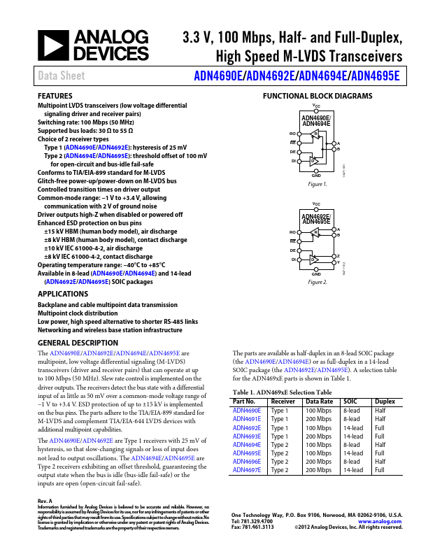
The ADN4690E/ADN4692E/ADN4694E/ADN4695E are multipoint, low voltage differential signaling (M-LVDS) transceivers (driver and receiver pairs) that can operate at up to 100 Mbps (50 MHz).

Slew rate control is implemented on the driver outputs.

Features

  • Multipoint LVDS transceivers (low voltage differential signaling driver and receiver pairs) Switching rate: 100 Mbps (50 MHz) Supported bus loads: 30 Ω to 55 Ω Choice of 2 receiver types Type 1 (ADN4690E/ADN4692E): hysteresis of 25 mV Type 2 (ADN4694E/ADN4695E): threshold offset of 100 mV for open-circuit and bus-idle fail-safe Conforms to TIA/EIA-899 standard for M-LVDS Glitch-free power-up/power-down on M-LVDS bus Controlled transition times on driver output Common-mode range:.
  • 1 V to.

📥 Download Datasheet

Note: The manufacturer provides a single datasheet file (ADN4694E_AnalogDevices.pdf) that lists specifications for multiple related part numbers.

Datasheet Details

Part number ADN4692E
Manufacturer Analog Devices
File Size 760.69 KB
Description (ADN4690E - ADN4695E) High Speed M-LVDS Transceivers
Datasheet download datasheet ADN4692E Datasheet
Other Datasheets by Analog Devices

Full PDF Text Transcription

Click to expand full text
3.3 V, 100 Mbps, Half- and Full-Duplex, High Speed M-LVDS Transceivers Data Sheet FEATURES Multipoint LVDS transceivers (low voltage differential signaling driver and receiver pairs) Switching rate: 100 Mbps (50 MHz) Supported bus loads: 30 Ω to 55 Ω Choice of 2 receiver types Type 1 (ADN4690E/ADN4692E): hysteresis of 25 mV Type 2 (ADN4694E/ADN4695E): threshold offset of 100 mV for open-circuit and bus-idle fail-safe Conforms to TIA/EIA-899 standard for M-LVDS Glitch-free power-up/power-down on M-LVDS bus Controlled transition times on driver output Common-mode range: −1 V to +3.
Published: |