Datasheet4U Logo Datasheet4U.com

ADA4625-2 - JFET Op Amp

This page provides the datasheet information for the ADA4625-2, a member of the ADA4625-1 JFET Op Amp family.

Description

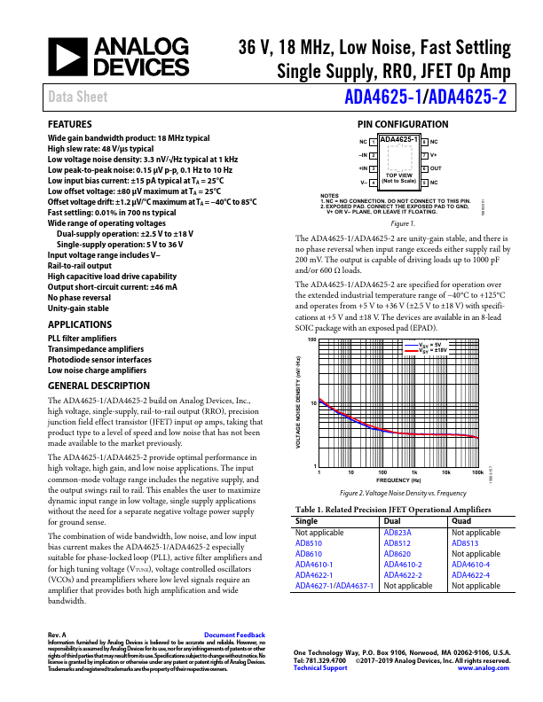
The ADA4625-1/ADA4625-2 build on Analog Devices, Inc., high voltage, single-supply, rail-to-rail output (RRO), precision junction field effect transistor (JFET) input op amps, taking that product type to a level of speed and low noise that has not been made available to the market previously.

Features

  • Wide gain bandwidth product: 18 MHz typical High slew rate: 48 V/µs typical Low voltage noise density: 3.3 nV/√Hz typical at 1 kHz Low peak-to-peak noise: 0.15 µV p-p, 0.1 Hz to 10 Hz Low input bias current: ±15 pA typical at TA = 25°C Low offset voltage: ±80 µV maximum at TA = 25°C Offset voltage drift: ±1.2 µV/°C maximum at TA =.
  • 40°C to 85°C Fast settling: 0.01% in 700 ns typical Wide range of operating voltages Dual-supply operation: ±2.5 V to ±18 V Single-supply operation: 5 V to 36.

📥 Download Datasheet

Datasheet preview – ADA4625-2

Datasheet Details

Part number ADA4625-2
Manufacturer Analog Devices
File Size 1.24 MB
Description JFET Op Amp
Datasheet download datasheet ADA4625-2 Datasheet
Additional preview pages of the ADA4625-2 datasheet.
Other Datasheets by Analog Devices

Full PDF Text Transcription

Click to expand full text
Data Sheet 36 V, 18 MHz, Low Noise, Fast Settling Single Supply, RRO, JFET Op Amp ADA4625-1/ADA4625-2 FEATURES Wide gain bandwidth product: 18 MHz typical High slew rate: 48 V/µs typical Low voltage noise density: 3.3 nV/√Hz typical at 1 kHz Low peak-to-peak noise: 0.15 µV p-p, 0.1 Hz to 10 Hz Low input bias current: ±15 pA typical at TA = 25°C Low offset voltage: ±80 µV maximum at TA = 25°C Offset voltage drift: ±1.2 µV/°C maximum at TA = −40°C to 85°C Fast settling: 0.01% in 700 ns typical Wide range of operating voltages Dual-supply operation: ±2.
Published: |