Datasheet Details
| Part number | AO9926 |
|---|---|
| Manufacturer | Alpha Industries |
| File Size | 234.80 KB |
| Description | Dual N-Channel MOSFET |
| Datasheet |
 AO9926 Datasheet AO9926 Datasheet
|
|
|
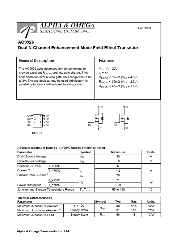
The AO9926 uses advanced trench technology to provide excellent RDS(ON) and low gate charge.
They offer operation over a wide gate drive range from 1.8V to 8V.
The two devices may be used individually, in parallel or to form a bidirectional blocking switch.
| Part number | AO9926 |
|---|---|
| Manufacturer | Alpha Industries |
| File Size | 234.80 KB |
| Description | Dual N-Channel MOSFET |
| Datasheet |
AO9926 Datasheet
|
|
|
|
| Part Number | Description | Manufacturer |
|---|---|---|
| AO9926A | Dual N-Channel MOSFET | ETC |
| AO9926B | 20V Dual N-Channel MOSFET | Alpha & Omega Semiconductors |
| AO9926E | Dual N-Channel MOSFET | Alpha & Omega Semiconductors |
| Part Number | Description |
|---|
The following content is an automatically extracted verbatim text from the original manufacturer datasheet and is provided for reference purposes only.