The following content is an automatically extracted verbatim text
from the original manufacturer datasheet and is provided for reference purposes only.
View original datasheet text
#
®
$65<)343
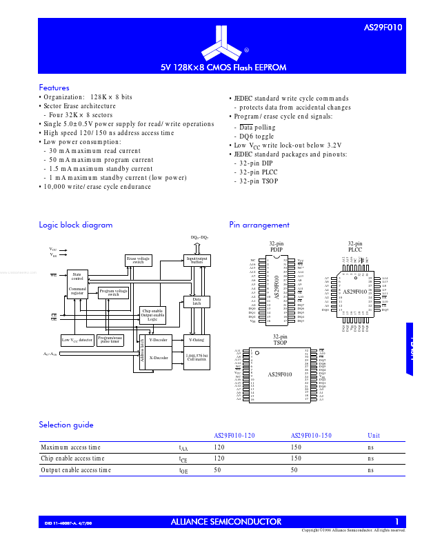
89#45;.ð;#&026#)ODVK#((3520 )HDWXUHV
• Organization: 128K × 8 bits • Sector Erase architecture - Four 32K × 8 sectors • Single 5.0±0.5V power supply for read/write operations • High speed 120/150 ns address access time • Low power consumption: - 30 mA maximum read current - 50 mA maximum program current - 1.5 mA maximum standby current - 1 mA maximum standby current (low power) • 10,000 write/erase cycle endurance • JEDEC standard write cycle commands - protects data from accidental changes • Program/erase cycle end signals: - Data polling - DQ6 toggle • Low VCC write lock-out below 3.
 AS29F010 Datasheet