Click to expand full text
ADV
ADM60N03E
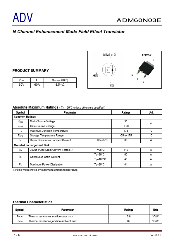
N-Channel Enhancement Mode Field Effect Transistor
PRODUCT SUMMARY
VDSS 60V
ID 60A
RDS(ON) (mΩ) 8.5mΩ
TO252
2
1 2 3
Absolute Maximum Ratings ( TA = 25°C unless otherwise specifed )
Symbol
Parameter
Ratings
Unit
Common Ratings
VDSS
Drain-Source Voltage
VGSS
Gate-Source Voltage
TJ
Maximum Junction Temperature
TSTG
Storage Temperature Range
IS
Diode Continuous Forward Current
30 V
±20
175
°C
-55 to 175
°C
TC=25°C
60
A
Mounted on Large Heat Sink
IDM
300μs Pulse Drain Current Tested⑴
TC=25°C
110
A
ID
Continuous Drain Current
TC=25°C
60
A
TC=100°C
40
A
PD
Maximum Power Dissipation
TC=25°C
41
W
1. Pulse width limited by maximum junction temperature.
 ADM60N03E Datasheet