Datasheet Details
| Part number | 74LVC3G34 |
|---|---|
| Manufacturer | Nexperia |
| File Size | 254.06 KB |
| Description | Triple buffer |
| Datasheet |
 74LVC3G34 Datasheet 74LVC3G34 Datasheet
|
|
|
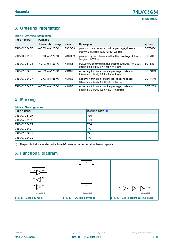
The 74LVC3G34 is a triple buffer.
Inputs can be driven from either 3.3 V or 5 V devices.
This feature allows the use of these devices as translators in mixed 3.3 V and 5 V environments.
| Part number | 74LVC3G34 |
|---|---|
| Manufacturer | Nexperia |
| File Size | 254.06 KB |
| Description | Triple buffer |
| Datasheet |
74LVC3G34 Datasheet
|
|
|
|
| Part Number | Description | Manufacturer |
|---|---|---|
| 74LVC3G34 | Triple buffer | NXP Semiconductors |
| 74LVC3G04 | Triple inverter | NXP |
| 74LVC3G04 | TRIPLE INVERTER GATE | DIODES |
| 74LVC3G06 | Triple inverter | NXP Semiconductors |
| 74LVC3G07 | Triple buffer | NXP Semiconductors |
| Part Number | Description |
|---|---|
| 74LVC3G34-Q100 | Triple buffer |
| 74LVC3G04 | Triple inverter |
| 74LVC3G04-Q100 | Triple inverter |
| 74LVC3G06 | Triple inverter |
| 74LVC3G07 | Triple buffer |
The following content is an automatically extracted verbatim text from the original manufacturer datasheet and is provided for reference purposes only.