Datasheet Summary
8-input NAND gate
Rev. 2
- 15 March 2019
Product data sheet
1. General description
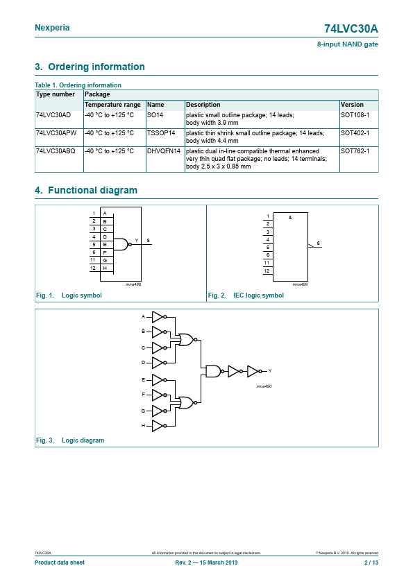
The 74LVC30A is an 8-input NAND gate.
Inputs can be driven from either 3.3 V or 5 V devices. This feature allows the use of these devices in a mixed 3.3 V and 5 V environment.
Schmitt trigger action at all inputs makes the circuit tolerant for slower input rise and fall time.
This device is fully specified for partial power-down applications using IOFF. The IOFF circuitry disables the output, preventing the damaging backflow current through the device when it is powered down.
2. Features and benefits
- Wide supply voltage range from 1.2 V to 3.6 V
- Inputs accept voltages up to 5.5 V
- CMOS low...