Datasheet Details
| Part number | 74LVC126A |
|---|---|
| Manufacturer | Nexperia |
| File Size | 269.27 KB |
| Description | Quad buffer/line driver |
| Datasheet |
 74LVC126A Datasheet 74LVC126A Datasheet
|
|
|
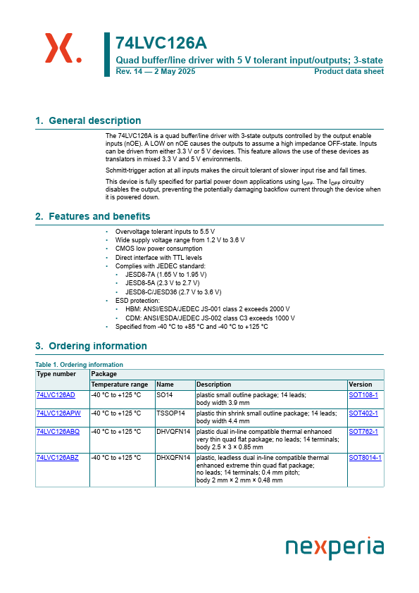
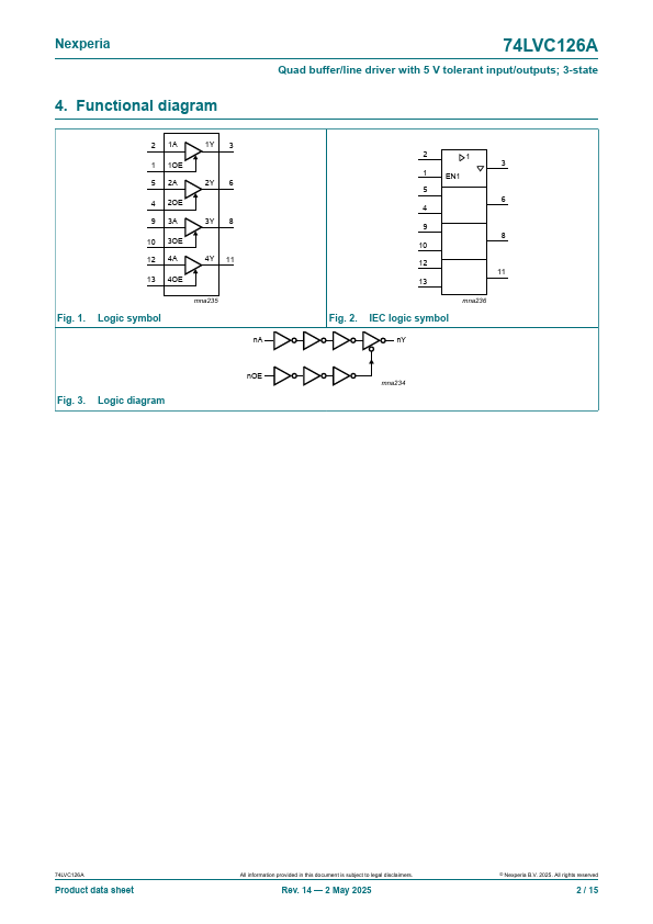
The 74LVC126A is a quad buffer/line driver with 3-state outputs controlled by the output enable inputs (nOE).
A LOW on nOE causes the outputs to assume a high impedance OFF-state.
Inputs can be driven from either 3.3 V or 5 V devices.
| Part number | 74LVC126A |
|---|---|
| Manufacturer | Nexperia |
| File Size | 269.27 KB |
| Description | Quad buffer/line driver |
| Datasheet |
74LVC126A Datasheet
|
|
|
|
| Part Number | Description | Manufacturer |
|---|---|---|
| 74LVC126A | Quad buffer/line driver | NXP |
| 74LVC126A | QUADRUPLE 3-STATE BUFFERS | Diodes |
| 74LVC126A | Low-Voltage CMOS Quad Buffer | ON Semiconductor |
| 74LVC126A | Quad Buffer | SG Micro |
| 74LVC125 | Quad buffer/line driver | Philips |
| Part Number | Description |
|---|---|
| 74LVC126A-Q100 | Quad buffer/line driver |
| 74LVC126AD | Quad buffer/line driver |
| 74LVC125A | Quad buffer/line driver |
| 74LVC125A-Q100 | Quad buffer/line driver |
| 74LVC10A | Triple 3-input NAND gate |
The following content is an automatically extracted verbatim text from the original manufacturer datasheet and is provided for reference purposes only.