Datasheet Details
| Part number | 74HCT74 |
|---|---|
| Manufacturer | Nexperia |
| File Size | 294.36 KB |
| Description | Dual D-type flip-flop |
| Datasheet |
 74HCT74 Datasheet 74HCT74 Datasheet
|
|
|
Download the 74HCT74 datasheet PDF. This datasheet also covers the 74HC74 variant, as both devices belong to the same dual d-type flip-flop family and are provided as variant models within a single manufacturer datasheet.
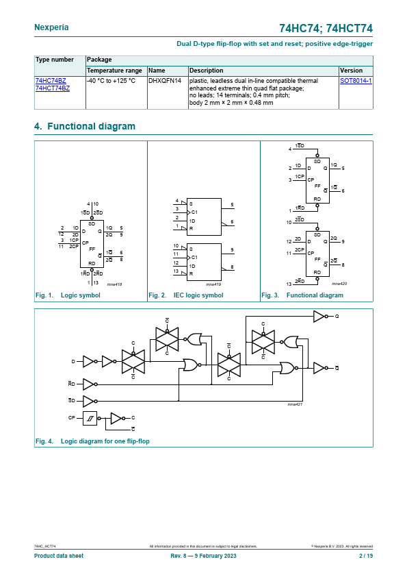
The 74HC74 and 74HCT74 are dual positive edge triggered D-type flip-flop.
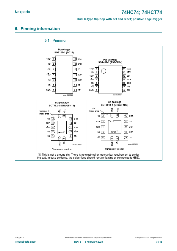
They have individual data (nD), clock (nCP), set (nSD) and reset (nRD) inputs, and complementary nQ and nQ outputs.
| Part number | 74HCT74 |
|---|---|
| Manufacturer | Nexperia |
| File Size | 294.36 KB |
| Description | Dual D-type flip-flop |
| Datasheet |
74HCT74 Datasheet
|
|
|
|
| Part Number | Description | Manufacturer |
|---|---|---|
| 74HCT74 | Dual D-Type Positive-Edge-Triggered Flip-Flips | Texas Instruments |
| 74HCT74 | Dual D-Type Flip-Flop | STMicroelectronics |
| 74HCT7403 | 4-Bit x 64-word FIFO register | Philips |
| 74HCT7403 | 4-bit x 64-word FIFO register | NXP |
| 74HCT7404 | 5-Bit x 64-word FIFO register | Philips |
| Part Number | Description |
|---|---|
| 74HCT74-Q100 | Dual D-type flip-flop |
| 74HCT74D | Dual D-type flip-flop |
| 74HCT7540 | Octal Schmitt trigger buffer/line driver |
| 74HCT7540D | Octal Schmitt trigger buffer/line driver |
| 74HCT7541 | Octal Schmitt trigger buffer/line driver |
The following content is an automatically extracted verbatim text from the original manufacturer datasheet and is provided for reference purposes only.