Datasheet Details
| Part number | 74HCT123D |
|---|---|
| Manufacturer | Nexperia |
| File Size | 317.40 KB |
| Description | Dual retriggerable monostable multivibrator |
| Datasheet |
 74HCT123D Datasheet 74HCT123D Datasheet
|
|
|
Download the 74HCT123D datasheet PDF. This datasheet also covers the 74HC123 variant, as both devices belong to the same dual retriggerable monostable multivibrator family and are provided as variant models within a single manufacturer datasheet.
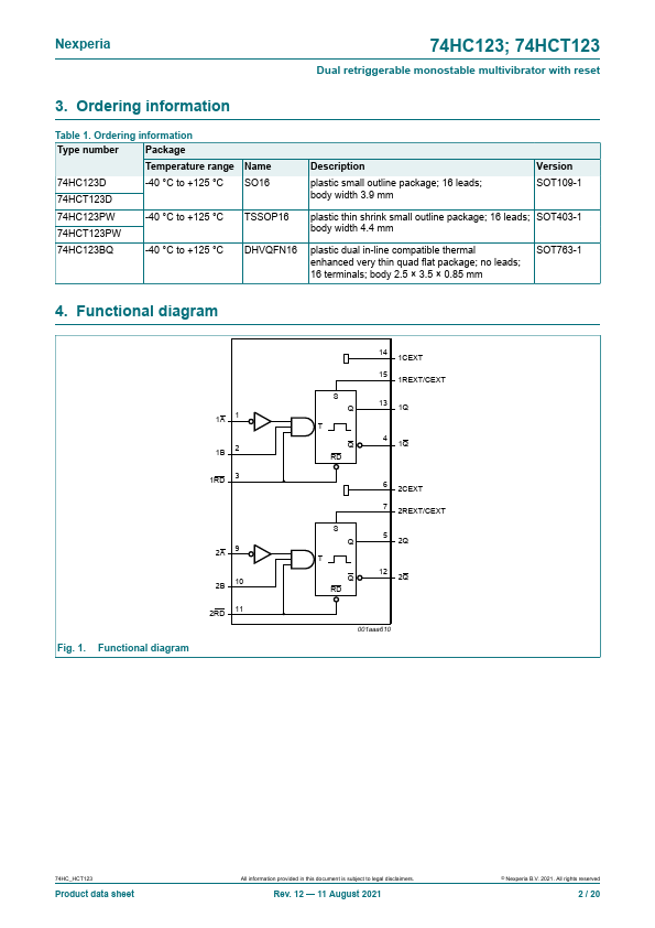
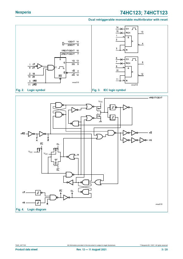
The 74HC123; 74HCT123 is a dual retriggerable monostable multivibrator with reset.
The basic output pulse width is programmed by selection of external components (REXT and CEXT).
Once triggered this basic pulse width may be extended by retriggering either of the edge triggered inputs (nA or nB).
| Part number | 74HCT123D |
|---|---|
| Manufacturer | Nexperia |
| File Size | 317.40 KB |
| Description | Dual retriggerable monostable multivibrator |
| Datasheet |
74HCT123D Datasheet
|
|
|
|
| Part Number | Description | Manufacturer |
|---|---|---|
| 74HCT123 | High-Speed CMOS Logic Dual Retriggerable Monostable Multivibrators | Texas Instruments |
| 74HCT123 | Dual retriggerable monostable multivibrator | Philips |
| 74HCT123 | Dual retriggerable monostable multivibrator | NXP |
| 74HCT123-Q100 | Dual retriggerable monostable multivibrator | NXP |
| 74HCT125 | QUADRUPLE 3-STATE BUFFERS | Diodes |
| Part Number | Description |
|---|---|
| 74HCT123DB | Dual retriggerable monostable multivibrator |
| 74HCT123 | Dual retriggerable monostable multivibrator |
| 74HCT123-Q100 | Dual retriggerable monostable multivibrator |
| 74HCT123PW | Dual retriggerable monostable multivibrator |
| 74HCT125 | Quad buffer/line driver |
The following content is an automatically extracted verbatim text from the original manufacturer datasheet and is provided for reference purposes only.