Datasheet Details
| Part number | 74HC3G34 |
|---|---|
| Manufacturer | Nexperia |
| File Size | 185.48 KB |
| Description | Triple buffer gate |
| Datasheet |
 74HC3G34 Datasheet 74HC3G34 Datasheet
|
|
|
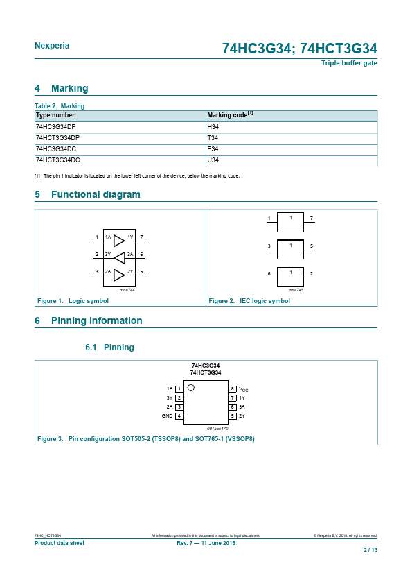
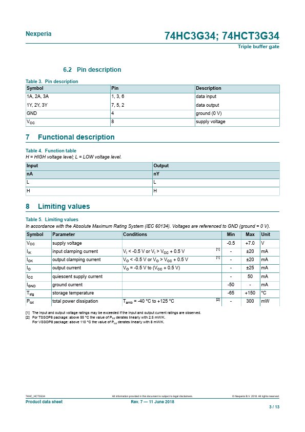
The 74HC3G34; 74HCT3G34 is a triple buffer.
Inputs include clamp diodes.
This enables the use of current limiting resistors to interface inputs to voltages in excess of VCC.
| Part number | 74HC3G34 |
|---|---|
| Manufacturer | Nexperia |
| File Size | 185.48 KB |
| Description | Triple buffer gate |
| Datasheet |
74HC3G34 Datasheet
|
|
|
|
| Part Number | Description | Manufacturer |
|---|---|---|
| 74HC3G34 | Triple Buffer Gate | NXP |
| 74HC3G04 | Inverter | NXP |
| 74HC3G06 | Triple inverter | NXP |
| 74HC3G07 | Buffer | NXP |
| 74HC3GU04 | Inverter | NXP |
| Part Number | Description |
|---|---|
| 74HC3G34-Q100 | Triple buffer gate |
| 74HC3G34DC | Triple buffer gate |
| 74HC3G34DP | Triple buffer gate |
| 74HC3G04 | Triple inverter |
| 74HC3G04-Q100 | Triple inverter |
The following content is an automatically extracted verbatim text from the original manufacturer datasheet and is provided for reference purposes only.