Datasheet Details
| Part number | 74HC259D |
|---|---|
| Manufacturer | Nexperia |
| File Size | 312.13 KB |
| Description | 8-bit addressable latch |
| Datasheet |
 74HC259D Datasheet 74HC259D Datasheet
|
|
|
Download the 74HC259D datasheet PDF. This datasheet also covers the 74HC259 variant, as both devices belong to the same 8-bit addressable latch family and are provided as variant models within a single manufacturer datasheet.
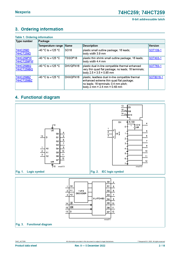
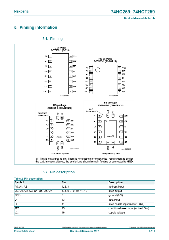
The 74HC259; 74HCT259 is an 8-bit addressable latch.
| Part number | 74HC259D |
|---|---|
| Manufacturer | Nexperia |
| File Size | 312.13 KB |
| Description | 8-bit addressable latch |
| Datasheet |
74HC259D Datasheet
|
|
|
|
| Part Number | Description | Manufacturer |
|---|---|---|
| 74HC259D | 8-Bit Addressable Latch | Toshiba |
| 74HC259 | 8-Bit Addressable Latches | Texas Instruments |
| 74HC251 | Data Selectors/Multiplexers | Texas Instruments |
| 74HC251 | 8-input multiplexer | Philips |
| 74HC253 | Dual 4-input multiplexer | Philips |
| Part Number | Description |
|---|---|
| 74HC259 | 8-bit addressable latch |
| 74HC259-Q100 | 8-bit addressable latch |
| 74HC251 | 8-input multiplexer |
| 74HC251-Q100 | 8-input multiplexer |
| 74HC251D | 8-input multiplexer |
The following content is an automatically extracted verbatim text from the original manufacturer datasheet and is provided for reference purposes only.