Datasheet Details
| Part number | 74AVC9112 |
|---|---|
| Manufacturer | Nexperia |
| File Size | 194.50 KB |
| Description | 1-to-4 fan-out buffer |
| Datasheet |
 74AVC9112 Datasheet 74AVC9112 Datasheet
|
|
|
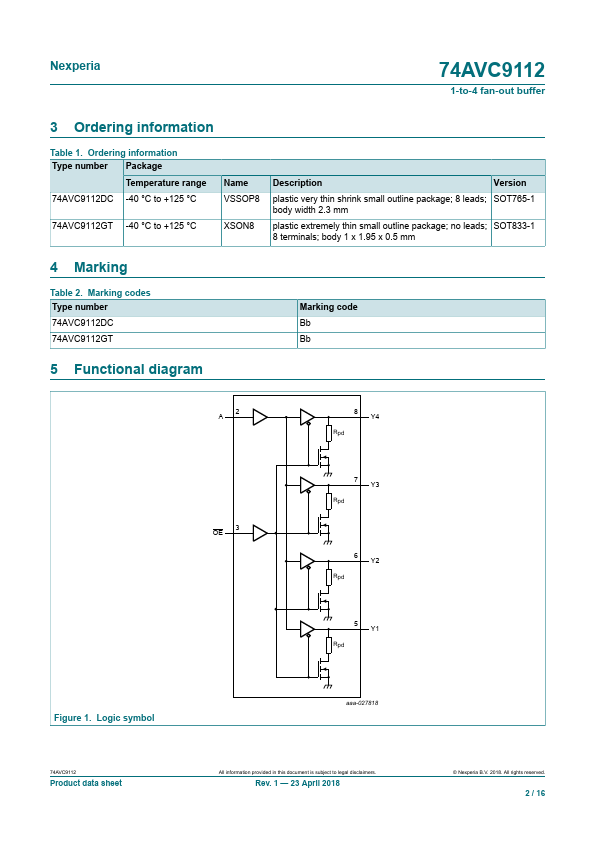
The 74AVC9112 is a 1-to-4 fan-out buffer suitable for use in clock distribution.
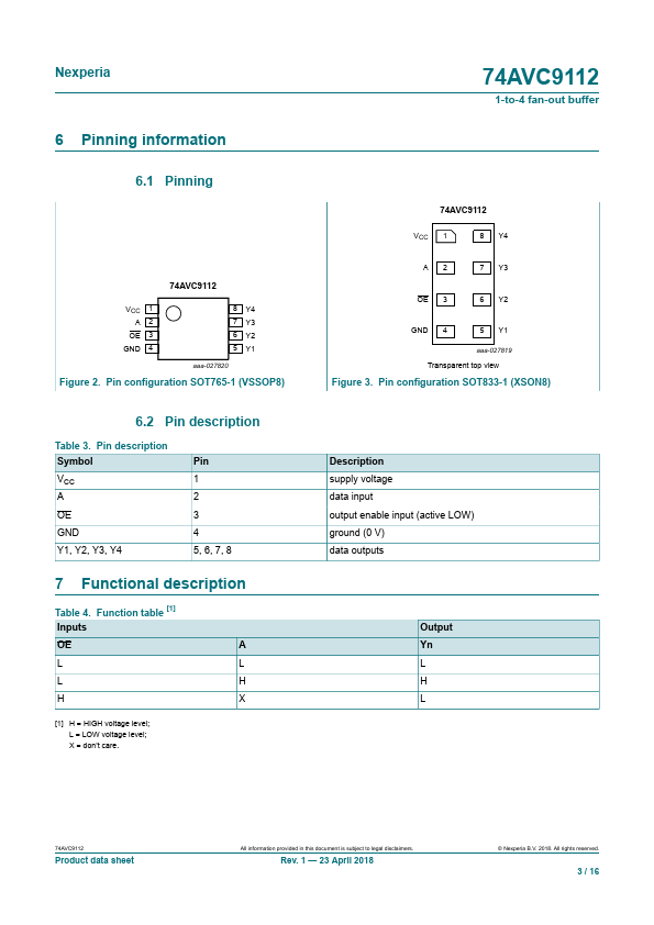
It has a data input (A), four data outputs (Yn) and an output enable input (OE).
VCC can be supplied at any voltage between 0.8 V and 3.6 V.
| Part number | 74AVC9112 |
|---|---|
| Manufacturer | Nexperia |
| File Size | 194.50 KB |
| Description | 1-to-4 fan-out buffer |
| Datasheet |
74AVC9112 Datasheet
|
|
|
|
| Part Number | Description | Manufacturer |
|---|---|---|
| 74AVC16244 | 16-bit buffer/line driver | NXP |
| 74AVC16245 | 16-bit transceiver | NXP |
| 74AVC16334A | 16-bit registered driver | NXP Semiconductors |
| 74AVC16373 | 16-bit D-type transparent latch | NXP |
| 74AVC16374 | 16-bit edge triggered D-type flip-flop | NXP |
| Part Number | Description |
|---|---|
| 74AVC16244 | 16-bit buffer/line driver |
| 74AVC16245 | 16-bit transceiver |
| 74AVC16245-Q100 | 16-bit transceiver |
| 74AVC16334A | 16-bit registered driver |
| 74AVC16373 | 16-bit D-type transparent latch |
The following content is an automatically extracted verbatim text from the original manufacturer datasheet and is provided for reference purposes only.