Datasheet Details
| Part number | 74AVC16835A |
|---|---|
| Manufacturer | Nexperia |
| File Size | 223.57 KB |
| Description | 18-bit registered driver |
| Datasheet |
 74AVC16835A Datasheet 74AVC16835A Datasheet
|
|
|
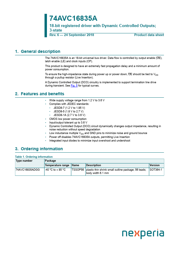
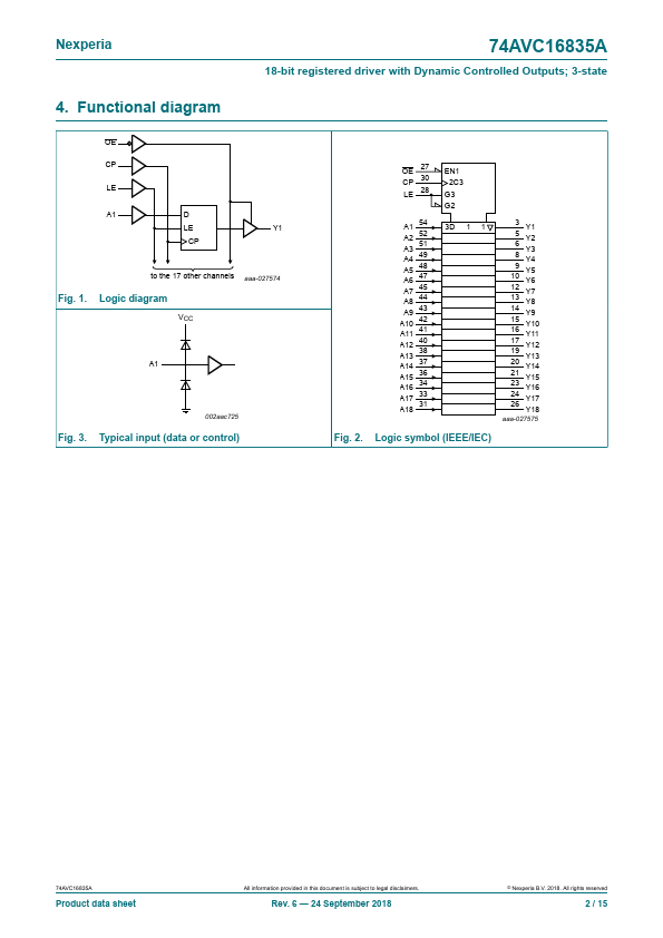
The 74AVC16835A is an 18-bit universal bus driver.
Data flow is controlled by output enable (OE), latch enable (LE) and clock inputs (CP).
This product is designed to have an extremely fast propagation delay and a minimum amount of power consumption.
| Part number | 74AVC16835A |
|---|---|
| Manufacturer | Nexperia |
| File Size | 223.57 KB |
| Description | 18-bit registered driver |
| Datasheet |
74AVC16835A Datasheet
|
|
|
|
| Part Number | Description | Manufacturer |
|---|---|---|
| 74AVC16835 | 18-bit registered driver | NXP |
| 74AVC16834 | 18-bit registered driver | NXP |
| 74AVC16836 | 20-bit registered driver | NXP |
| 74AVC16836A | 20-bit registered driver | NXP |
| 74AVC16244 | 16-bit buffer/line driver | NXP |
| Part Number | Description |
|---|---|
| 74AVC16834A | 18-bit registered driver |
| 74AVC16836A | 20-bit registered driver |
| 74AVC16244 | 16-bit buffer/line driver |
| 74AVC16245 | 16-bit transceiver |
| 74AVC16245-Q100 | 16-bit transceiver |
The following content is an automatically extracted verbatim text from the original manufacturer datasheet and is provided for reference purposes only.