Datasheet Details
| Part number | 74AUP2G07 |
|---|---|
| Manufacturer | Nexperia |
| File Size | 256.34 KB |
| Description | Low-power dual buffer |
| Datasheet |
 74AUP2G07 Datasheet 74AUP2G07 Datasheet
|
|
|
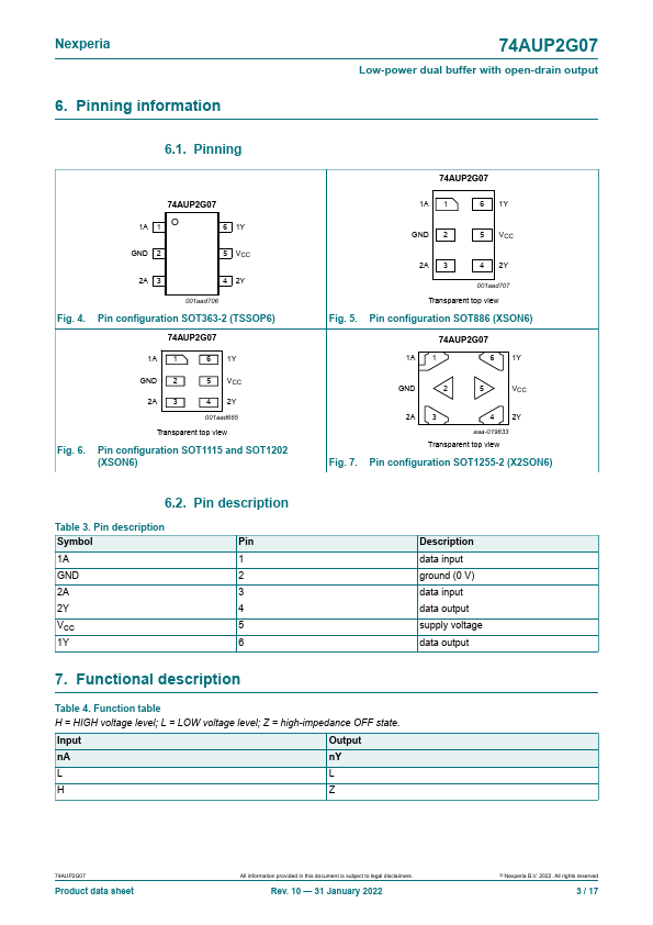
The 74AUP2G07 is a dual buffer with open-drain outputs.
Schmitt-trigger action at all inputs makes the circuit tolerant of slower input rise and fall times.
This device ensures very low static and dynamic power consumption across the entire VCC range from 0.8 V to 3.6 V.
| Part number | 74AUP2G07 |
|---|---|
| Manufacturer | Nexperia |
| File Size | 256.34 KB |
| Description | Low-power dual buffer |
| Datasheet |
74AUP2G07 Datasheet
|
|
|
|
| Part Number | Description | Manufacturer |
|---|---|---|
| 74AUP2G07 | Low-power dual buffer | NXP Semiconductors |
| 74AUP2G07 | DUAL BUFFERS | Diodes |
| 74AUP2G00 | Low-power dual 2-input NAND gate | NXP |
| 74AUP2G00 | DUAL NAND GATE | Diodes |
| 74AUP2G02 | DUAL NOR GATE | Diodes |
| Part Number | Description |
|---|---|
| 74AUP2G00 | Low-power dual 2-input NAND gate |
| 74AUP2G00-Q100 | Low-power dual 2-input NAND gate |
| 74AUP2G02 | Low-power dual 2-input NOR gate |
| 74AUP2G04 | Low-power dual inverter |
| 74AUP2G04-Q100 | Low-power dual inverter |
The following content is an automatically extracted verbatim text from the original manufacturer datasheet and is provided for reference purposes only.