Datasheet Details
| Part number | 74AUP1G07 |
|---|---|
| Manufacturer | Nexperia |
| File Size | 268.03 KB |
| Description | Low-power buffer |
| Datasheet |
 74AUP1G07 Datasheet 74AUP1G07 Datasheet
|
|
|
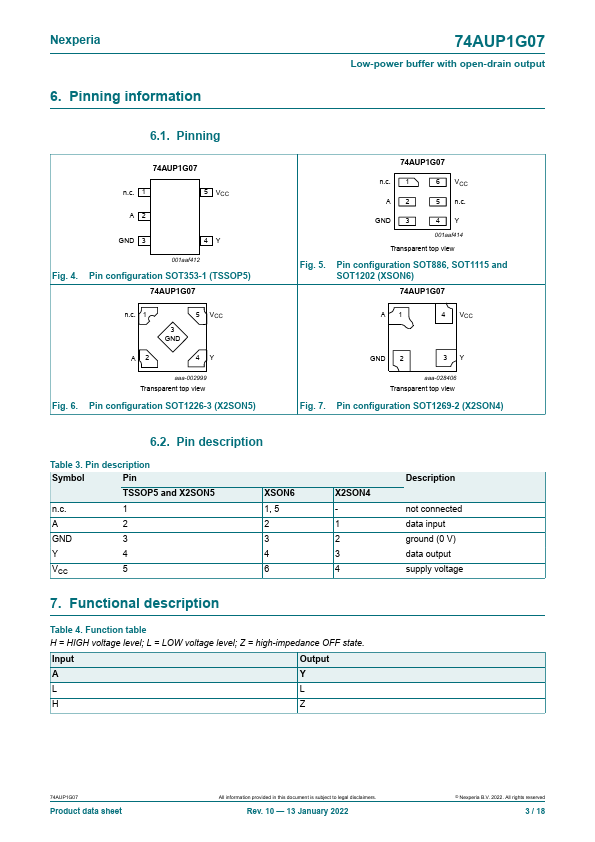
The 74AUP1G07 is a single buffer with open-drain output.
Schmitt-trigger action at all inputs makes the circuit tolerant of slower input rise and fall times.
This device ensures a very low static and dynamic power consumption across the entire VCC range from 0.8 V to 3.6 V.
| Part number | 74AUP1G07 |
|---|---|
| Manufacturer | Nexperia |
| File Size | 268.03 KB |
| Description | Low-power buffer |
| Datasheet |
74AUP1G07 Datasheet
|
|
|
|
| Part Number | Description | Manufacturer |
|---|---|---|
| 74AUP1G07 | Low-power buffer | NXP Semiconductors |
| 74AUP1G07 | SINGLE BUFFER/DRIVER | Diodes |
| 74AUP1G00 | Low-power 2-input NAND gate | NXP Semiconductors |
| 74AUP1G00 | SINGLE 2 INPUT POSITIVE NAND GATE | Diodes |
| 74AUP1G02 | Low-power 2-input NOR gate | NXP |
| Part Number | Description |
|---|---|
| 74AUP1G07-Q100 | Low-power buffer |
| 74AUP1G00 | Low-power 2-input NAND gate |
| 74AUP1G00-Q100 | Low-power 2-input NAND gate |
| 74AUP1G02 | Low-power 2-input NOR gate |
| 74AUP1G02-Q100 | Low-power 2-input NOR gate |
The following content is an automatically extracted verbatim text from the original manufacturer datasheet and is provided for reference purposes only.