74ALVCH16952DGG Description
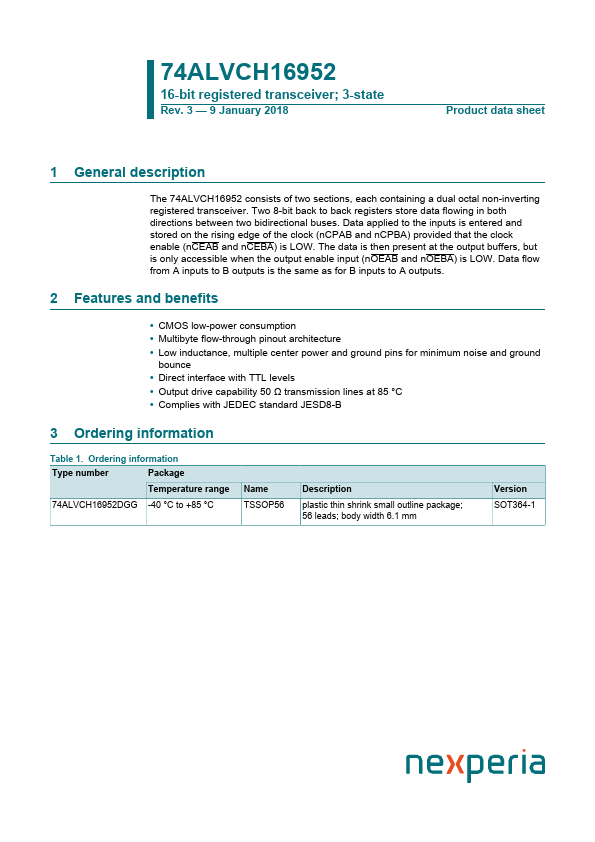
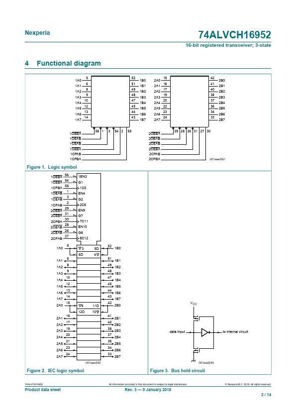
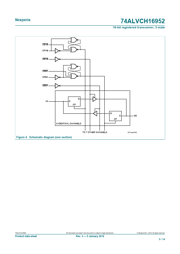
The 74ALVCH16952 consists of two sections, each containing a dual octal non-inverting registered transceiver. Two 8-bit back to back registers store data flowing in both directions between two bidirectional buses. Data applied to the inputs is entered and stored on the rising edge of the clock (nCPAB and nCPBA) provided that the clock enable (nCEAB and nCEBA) is LOW.
74ALVCH16952DGG Key Features
- CMOS low-power consumption
- Multibyte flow-through pinout architecture
- Low inductance, multiple center power and ground pins for minimum noise and ground
- Direct interface with TTL levels
- Output drive capability 50 Ω transmission lines at 85 °C
- plies with JEDEC standard JESD8-B
- 9 January 2018
- 9 January 2018