TPS65132 Overview
Key Specifications
Mount Type: Surface Mount
Pins: 15
Operating Voltage: 5.5 V
Height: 625 µm
Description
The TPS65132 family is designed to supply positive/negative driven applications. The device uses a single inductor scheme for both outputs to provide the user smallest solution size, a small bill-of-material as well as high efficiency.
Key Features
- 1 Input Voltage Range: 2.5 V to 5.5 V
- VPOS Boost Converter: 4 V to 6 V (0.1-V step)
- VNEG Inverting Buck-Boost Converter: –6 V to –4 V (0.1-V step)
- Maximum Output Current: 80 mA or 150 mA
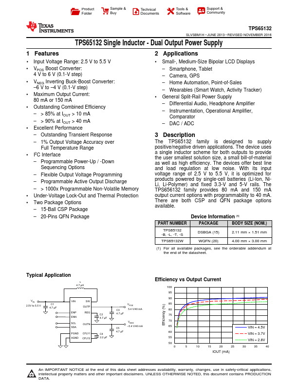
- Outstanding Combined Efficiency – > 85% at IOUT > 10 mA – > 90% at IOUT > 40 mA