TPS51206
Overview
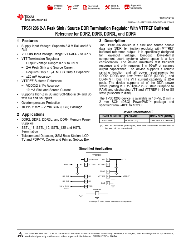
The TPS51206 device is a sink and source double date rate (DDR) termination regulator with VTTREF buffered reference output. It is specifically designed for low-input voltage, low-cost, low-external component count systems where space is a key consideration.
- 1 Supply Input Voltage: Supports 3.3-V Rail and 5-V Rail
- VLDOIN Input Voltage Range: VTT+0.4 V to 3.5 V
- VTT Termination Regulator - Output Voltage Range: 0.5 V to 0.9 V - 2-A Peak Sink and Source Current - Requires Only 10-μF MLCC Output Capacitor - ±20 mV Accuracy
- VTTREF Buffered Reference - VDDQ/2 ± 1% Accuracy - 10-mA Sink and Source Current
- Supports High-Z in S3 and Soft-Stop in S4 and S5 with S3 and S5 Inputs
- Overtemperature Protection
- 10-Pin, 2 mm × 2 mm SON (DSQ) Package